- 您現(xiàn)在的位置:買(mǎi)賣(mài)IC網(wǎng) > PDF目錄384654 > MAX1889ETE (MAXIM INTEGRATED PRODUCTS INC) Triple-Output TFT LCD Power Supply with Fault Protection PDF資料下載
參數(shù)資料
| 型號(hào): | MAX1889ETE |
| 廠(chǎng)商: | MAXIM INTEGRATED PRODUCTS INC |
| 元件分類(lèi): | 穩(wěn)壓器 |
| 英文描述: | Triple-Output TFT LCD Power Supply with Fault Protection |
| 中文描述: | 2.8 A SWITCHING REGULATOR, 1250 kHz SWITCHING FREQ-MAX, QCC16 |
| 封裝: | 5 X 5 MM, 0.80 MM HEIGHT, ULTRA THIN, QFN-16 |
| 文件頁(yè)數(shù): | 19/32頁(yè) |
| 文件大?。?/td> | 796K |
| 代理商: | MAX1889ETE |
第1頁(yè)第2頁(yè)第3頁(yè)第4頁(yè)第5頁(yè)第6頁(yè)第7頁(yè)第8頁(yè)第9頁(yè)第10頁(yè)第11頁(yè)第12頁(yè)第13頁(yè)第14頁(yè)第15頁(yè)第16頁(yè)第17頁(yè)第18頁(yè)當(dāng)前第19頁(yè)第20頁(yè)第21頁(yè)第22頁(yè)第23頁(yè)第24頁(yè)第25頁(yè)第26頁(yè)第27頁(yè)第28頁(yè)第29頁(yè)第30頁(yè)第31頁(yè)第32頁(yè)
M
Triple-Output TFT LCD Power Supply
with Fault Protection
______________________________________________________________________________________
19
Input Capacitor
The input capacitor (C
IN
) reduces the current peaks
drawn from the input supply and reduces noise injection
into the device. Two 3.3μF ceramic capacitors are used
in the standard application circuit (Figure 1) because of
the high source impedance seen in typical lab setups.
Actual applications usually have much lower source
impedance since the step-up regulator typically runs
directly from the output of another regulated supply.
Typically, C
IN
can be reduced below the values used in
the standard applications circuit. Ensure a low noise sup-
ply at the IN pin by using adequate C
IN
. Alternatively,
greater voltage variation can be tolerated on C
IN
if IN is
decoupled from C
IN
using an RC lowpass filter (see R1,
C1 in Figure 1).
Rectifier Diode
The MAX1889
’
s high switching frequency demands a
high-speed rectifier. Schottky diodes are recommend-
ed for most applications because of their fast recovery
time and low forward voltage. In general, a 1A Schottky
diode complements the internal MOSFET well.
Input P-Channel MOSFET
Select the input P-channel MOSFET based on the cur-
rent rating, voltage rating, gate threshold, and on-resis-
tance. The MOSFET must be able to handle the peak
input current (see the
Inductor Selection
section). The
drain-to-source voltage rating of the input MOSFET
should be higher than the maximum input voltage.
Because the MOSFET conducts the full input current,
the on-resistance should be low enough for higher effi-
ciency. Use a low-threshold MOSFET to ensure that the
switch is fully enhanced at lowest input voltages.
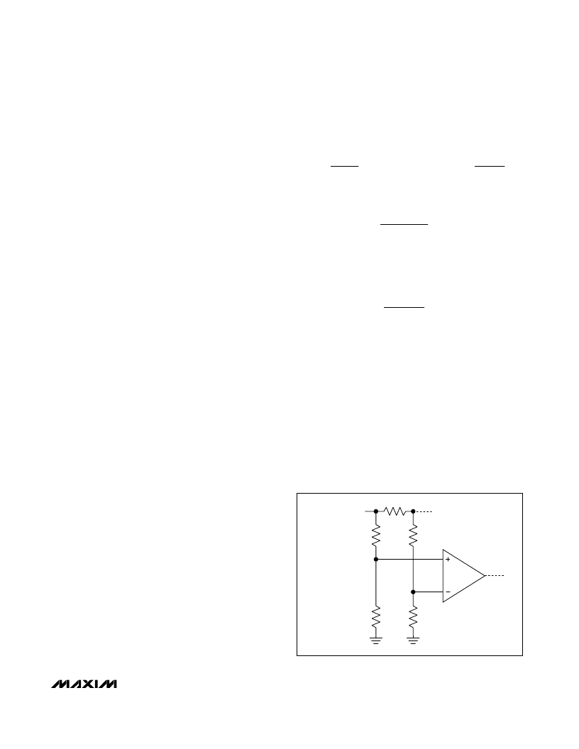
Setting the Input Overcurrent Threshold
The high-side comparator of the MAX1889 provides
input overcurrent protection when used in conjunction
with an external P-channel MOSFET P1. The accuracy
of the overcurrent threshold is affected by many fac-
tors, including comparator offset, resistor tolerance,
input voltage range, and variations in MOSFET
R
DS(ON)
. The input overcurrent comparator is only
intended to protect against catastrophic failures. This
function is similar to an input fuse.
To minimize the impact of the comparator
’
s input offset
on the current-sense accuracy, the sense voltage
should be close to the upper limit of the common-mode
range, which extends up to 80% of the input voltage.
The resistive voltage-divider (R3/R4), combined with
the on-state resistance of P1, sets the overcurrent
threshold. The center of R3/R4 is connected to the
inverting input (OCN) as shown in Figure 6.
If the comparator and resistors are ideal, the threshold
is at the current where both inputs are equal:
I
L(MAX)
is the average inductor current at maximum load
condition and minimum input voltage, and given by:
where
η
is the efficiency of the main step-up regulator.
If the step-up regulator
’
s minimum input voltage is 2.7V,
output voltage is 9V and maximum load current is 0.3A.
Assuming 80% efficiency, the maximum average induc-
tor current is:
V
L MAX
(
)
.
0 8 2 7
R
DS(MAX)
is the maximum on-state drain-to-source
resistance of P1. The maximum R
DS(ON)
at +25
°
C can
be found in the MOSFET data sheet, but that number
does not include the temperature coefficient.
Since the temperature coefficient for the resistance is
0.5%/
°
C, R
DS(MAX)
can be calculated with the following
equation:
where T
J
is the actual MOSFET junction temperature in
normal operation due to ambient temperature rise and
self-heating caused by power dissipation. As an exam-
ple, consider Fairchild FDN304P, which has a maxi-
mum R
DS(ON)
at room temperature of 70m
.
R
R
T
DS MAX
(
DS
C
J
)
_
.
=
×
×
(
)
[
]
°
25
1 0 005
25
-
I
V
A
A
.
.
.
=
×
=
9
0 3
1 25
I
V
V
I
L MAX
(
OUT
IN MIN
(
LOAD MAX
)
)
(
)
=
×
×
η
V
R
+
1
R
R
V
I
R
R
R
R
IN
IN
L MAX
-
(
DS MAX
(
×
=
×
(
)
×
+
2
2
4
3
4
)
)
V
IN
R
DS(ON)
R1
R2
R3
R4
OCP
OCN
OC COMP
Figure 6. Setting the Overcurrent Threshold
相關(guān)PDF資料 |
PDF描述 |
|---|---|
| MAX1889 | Fixed-Point Digital Signal Processor 256-BGA |
| MAX1896 | 1.4MHz SOT23 Current-Mode Step-Up DC-DC Converter |
| MAX1896EUT-T | Fixed-Point Digital Signal Processor 532-FCBGA |
| MAX1898 | Fixed-Point Digital Signal Processor 532-FCBGA |
| MAX1898EUB41 | Linear Charger for Single-Cell Li Battery |
相關(guān)代理商/技術(shù)參數(shù) |
參數(shù)描述 |
|---|---|
| MAX1889ETE+ | 功能描述:直流/直流開(kāi)關(guān)轉(zhuǎn)換器 Quad-Output TFT LCD Power Supply RoHS:否 制造商:STMicroelectronics 最大輸入電壓:4.5 V 開(kāi)關(guān)頻率:1.5 MHz 輸出電壓:4.6 V 輸出電流:250 mA 輸出端數(shù)量:2 最大工作溫度:+ 85 C 安裝風(fēng)格:SMD/SMT |
| MAX1889ETE+T | 功能描述:LCD 驅(qū)動(dòng)器 Quad-Output TFT LCD Power Supply RoHS:否 制造商:Maxim Integrated 數(shù)位數(shù)量:4.5 片段數(shù)量:30 最大時(shí)鐘頻率:19 KHz 工作電源電壓:3 V to 3.6 V 最大工作溫度:+ 85 C 最小工作溫度:- 20 C 封裝 / 箱體:PDIP-40 封裝:Tube |
| MAX1889ETE-T | 功能描述:LCD 驅(qū)動(dòng)器 RoHS:否 制造商:Maxim Integrated 數(shù)位數(shù)量:4.5 片段數(shù)量:30 最大時(shí)鐘頻率:19 KHz 工作電源電壓:3 V to 3.6 V 最大工作溫度:+ 85 C 最小工作溫度:- 20 C 封裝 / 箱體:PDIP-40 封裝:Tube |
| MAX1889EVKIT | 功能描述:電源管理IC開(kāi)發(fā)工具 MAX1889 Eval Kit RoHS:否 制造商:Maxim Integrated 產(chǎn)品:Evaluation Kits 類(lèi)型:Battery Management 工具用于評(píng)估:MAX17710GB 輸入電壓: 輸出電壓:1.8 V |
| MAX188ACAP | 功能描述:模數(shù)轉(zhuǎn)換器 - ADC Integrated Circuits (ICs) RoHS:否 制造商:Texas Instruments 通道數(shù)量:2 結(jié)構(gòu):Sigma-Delta 轉(zhuǎn)換速率:125 SPs to 8 KSPs 分辨率:24 bit 輸入類(lèi)型:Differential 信噪比:107 dB 接口類(lèi)型:SPI 工作電源電壓:1.7 V to 3.6 V, 2.7 V to 5.25 V 最大工作溫度:+ 85 C 安裝風(fēng)格:SMD/SMT 封裝 / 箱體:VQFN-32 |
發(fā)布緊急采購(gòu),3分鐘左右您將得到回復(fù)。