- 您現(xiàn)在的位置:買賣IC網(wǎng) > PDF目錄358870 > LM5112-SDX (NATIONAL SEMICONDUCTOR CORP) Tiny 7A MOSFET Gate Driver PDF資料下載
參數(shù)資料
| 型號(hào): | LM5112-SDX |
| 廠商: | NATIONAL SEMICONDUCTOR CORP |
| 元件分類: | MOSFETs |
| 英文描述: | Tiny 7A MOSFET Gate Driver |
| 中文描述: | 7 A BUF OR INV BASED MOSFET DRIVER, DSO6 |
| 封裝: | 3 X 3 MM, LLP-6 |
| 文件頁(yè)數(shù): | 8/10頁(yè) |
| 文件大小: | 236K |
| 代理商: | LM5112-SDX |
Layout Considerations
Attention must be given to board layout when using LM5112.
Some important considerations include:
1.
A Low ESR/ESL capacitor must be connected close to
the IC and between the V
and V
EE
pins to support
high peak currents being drawn from V
CC
during turn-on
of the MOSFET.
2.
Proper grounding is crucial. The driver needs a very low
impedance path for current return to ground avoiding
inductive loops. Two paths for returning current to
ground are a) between LM5112 IN_REF pin and the
ground of the circuit that controls the driver inputs and b)
between LM5112 V
EE
pin and the source of the power
MOSFET being driven. Both paths should be as short as
possible to reduce inductance and be as wide as pos-
sible to reduce resistance. These ground paths should
be distinctly separate to avoid coupling between the high
current output paths and the logic signals that drive the
LM5112. With rise and fall times in the range of 10 to
30nsec, care is required to minimize the lengths of cur-
rent carrying conductors to reduce their inductance and
EMI from the high di/dt transients generated when driv-
ing large capacitive loads.
3.
If either channel is not being used, the respective input
pin (IN or INB) should be connected to either V
EE
or V
CC
to avoid spurious output signals.
Thermal Performance
INTRODUCTION
The primary goal of the thermal management is to maintain
the integrated circuit (IC) junction temperature (Tj) below a
specified limit to ensure reliable long term operation. The
maximum T
J
of IC components should be estimated in worst
case operating conditions. The junction temperature can be
calculated based on the power dissipated on the IC and the
junction to ambient thermal resistance
θ
JA
for the IC pack-
age in the application board and environment. The
θ
JA
is not
a given constant for the package and depends on the PCB
design and the operating environment.
DRIVE POWER REQUIREMENT CALCULATIONS IN
LM5112
LM5112 is a single low side MOSFET driver capable of
sourcing / sinking 3A / 7A peak currents for short intervals to
drive a MOSFET without exceeding package power dissipa-
tion limits. High peak currents are required to switch the
MOSFET gate very quickly for operation at high frequencies.
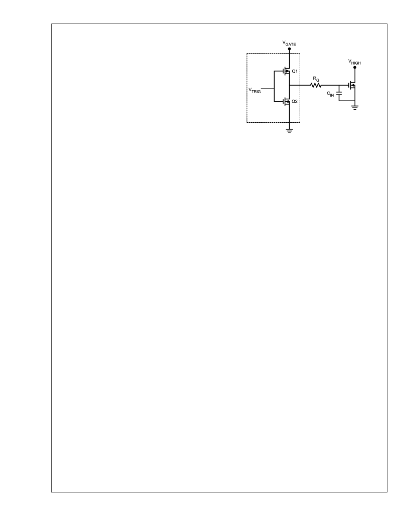
The schematic above shows a conceptual diagram of the
LM5112 output and MOSFET load. Q1 and Q2 are the
switches within the gate driver. Rg is the gate resistance of
the external MOSFET, and Cin is the equivalent gate capaci-
tance of the MOSFET. The equivalent gate capacitance is a
difficult parameter to measure as it is the combination of Cgs
(gate to source capacitance) and Cgd (gate to drain capaci-
tance). The Cgd is not a constant and varies with the drain
voltage. The better way of quantifying gate capacitance is
the gate charge Qg in coloumbs. Qg combines the charge
required by Cgs and Cgd for a given gate drive voltage
Vgate. The gate resistance Rg is usually very small and
losses in it can be neglected. The total power dissipated in
the MOSFET driver due to gate charge is approximated by:
P
DRIVER
= V
GATE
x Q
G
x F
SW
Where
F
SW
= switching frequency of the MOSFET.
For example, consider the MOSFET MTD6N15 whose gate
charge specified as 30 nC for V
GATE
= 12V.
Therefore, the power dissipation in the driver due to charging
and discharging of MOSFET gate capacitances at switching
frequency of 300 kHz and V
GATE
of 12V is equal to
P
DRIVER
= 12V x 30 nC x 300 kHz = 0.108W.
In addition to the above gate charge power dissipation, -
transient power is dissipated in the driver during output
transitions. When either output of the LM5112 changes state,
current will flow from V
CC
to V
EE
for a very brief interval of
time through the output totem-pole N and P channel
MOSFETs. The final component of power dissipation in the
driver is the power associated with the quiescent bias cur-
rent consumed by the driver input stage and Under-voltage
lockout sections.
Characterization of the LM5112 provides accurate estimates
of the transient and quiescent power dissipation compo-
nents. At 300 kHz switching frequency and 30 nC load used
in the example, the transient power will be 8 mW. The 1 mA
nominal quiescent current and 12V V
GATE
supply produce a
12 mW typical quiescent power.
Therefore the total power dissipation
P
D
= 0.118 + 0.008 + 0.012 = 0.138W.
We know that the junction temperature is given by
T
J
= P
D
x
θ
JA
+ T
A
Or the rise in temperature is given by
T
RISE
= T
J
T
A
= P
D
x
θ
JA
20066806
FIGURE 3.
L
www.national.com
8
相關(guān)PDF資料 |
PDF描述 |
|---|---|
| LM5115 | Secondary Side Post Regulator Controller |
| LM5115SD | Secondary Side Post Regulator Controller |
| LM5115SDX | Secondary Side Post Regulator Controller |
| LM5115MM | Secondary Side Post Regulator Controller |
| LM5115MMX | Secondary Side Post Regulator Controller |
相關(guān)代理商/技術(shù)參數(shù) |
參數(shù)描述 |
|---|---|
| LM5112SDX/NOPB | 功能描述:功率驅(qū)動(dòng)器IC RoHS:否 制造商:Micrel 產(chǎn)品:MOSFET Gate Drivers 類型:Low Cost High or Low Side MOSFET Driver 上升時(shí)間: 下降時(shí)間: 電源電壓-最大:30 V 電源電壓-最小:2.75 V 電源電流: 最大功率耗散: 最大工作溫度:+ 85 C 安裝風(fēng)格:SMD/SMT 封裝 / 箱體:SOIC-8 封裝:Tube |
| LM5113 | 制造商:TI 制造商全稱:Texas Instruments 功能描述:LM5113 5A, 100V Half-Bridge Gate Driver for Enhancement Mode GaN FETs |
| LM5113_1211 | 制造商:TI 制造商全稱:Texas Instruments 功能描述:LM5113 5A, 100V Half-Bridge Gate Driver for Enhancement Mode GaN FETs |
| LM5113LLPEVB/NOPB | 功能描述:電源管理IC開(kāi)發(fā)工具 LM5113 Eval Brd RoHS:否 制造商:Maxim Integrated 產(chǎn)品:Evaluation Kits 類型:Battery Management 工具用于評(píng)估:MAX17710GB 輸入電壓: 輸出電壓:1.8 V |
| LM5113SD | 制造商:TI 制造商全稱:Texas Instruments 功能描述:LM5113 5A, 100V Half-Bridge Gate Driver for Enhancement Mode GaN FETs |
發(fā)布緊急采購(gòu),3分鐘左右您將得到回復(fù)。