- 您現(xiàn)在的位置:買賣IC網(wǎng) > PDF目錄98000 > LLT3837EFE (LINEAR TECHNOLOGY CORP) SWITCHING CONTROLLER, 110 kHz SWITCHING FREQ-MAX, PDSO16 PDF資料下載
參數(shù)資料
| 型號(hào): | LLT3837EFE |
| 廠商: | LINEAR TECHNOLOGY CORP |
| 元件分類: | 穩(wěn)壓器 |
| 英文描述: | SWITCHING CONTROLLER, 110 kHz SWITCHING FREQ-MAX, PDSO16 |
| 封裝: | 4.40 MM, PLASTIC, TSSOP-16 |
| 文件頁(yè)數(shù): | 17/28頁(yè) |
| 文件大小: | 255K |
| 代理商: | LLT3837EFE |
第1頁(yè)第2頁(yè)第3頁(yè)第4頁(yè)第5頁(yè)第6頁(yè)第7頁(yè)第8頁(yè)第9頁(yè)第10頁(yè)第11頁(yè)第12頁(yè)第13頁(yè)第14頁(yè)第15頁(yè)第16頁(yè)當(dāng)前第17頁(yè)第18頁(yè)第19頁(yè)第20頁(yè)第21頁(yè)第22頁(yè)第23頁(yè)第24頁(yè)第25頁(yè)第26頁(yè)第27頁(yè)第28頁(yè)
LT3837
24
3837fa
APPLICATIONS INFORMATION
The other 1% is due to the bulk C component, so use:
C
I
Vf
OUT
OSC
≥
1%
In many applications the output capacitor is created from
multiple capacitors to achieve desired voltage ripple, reli-
ability and cost goals. For example, a low ESR ceramic
capacitor can minimize the ESR step, while an electrolytic
capacitor satises the required bulk C.
Continuing our example, the output capacitor needs:
ESR
V
A
m
C
A
COUT
OUT
≤
()
=Ω
≥
1
33
1 524
10
16
10
1
%
.
–
. %
.
%
% .
3 3 200
1515
kHz
F
=μ
These electrical characteristics require paralleling several
low ESR capacitors possibly of mixed type.
Most capacitor ripple current ratings are based on 2000
hour life. This makes it advisable to derate the capacitor
or to choose a capacitor rated at a higher temperature
than required.
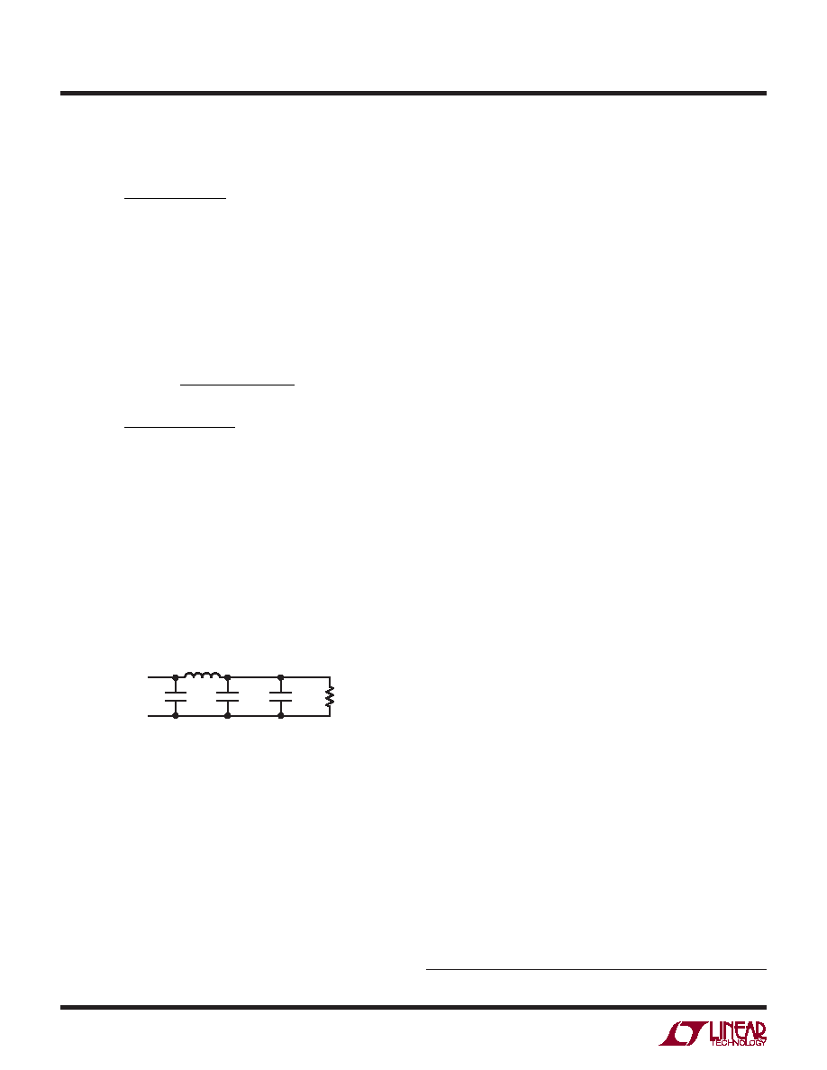
One way to reduce cost and improve output ripple is to
use a simple LC lter. Figure 8 shows an example of the
lter.
RLOAD
COUT2
1μF
VOUT
COUT
470μF
C1
47μF
3
FROM
SECONDARY
WINDING
L1
0.1μH
3837 F08
Figure 8
The design of the lter is beyond the scope of this data
sheet. However, as a starting point, use these general
guide lines. Start with a COUT 1/4 the size of the nonlter
solution. Make C1 1/4 of COUT to make the second lter
pole independent of COUT. The smaller C1 may be best
implemented with multiple ceramic capacitors. Make L1
smaller than the output inductance of the transformer. In
general, a 0.1
μH lter inductor is sufcient. Add a small
ceramic capacitor (COUT2)forhighfrequencynoiseonVOUT.
For those interested in more details refer to “Second-Stage
LC Filter Design,” Ridley, Switching Power Magazine, July
2000, p8-10.
Circuit simulation is a way to optimize output capacitance
and lters, just make sure to include the component
parasitics. LTC SwitcherCAD is a terric free circuit
simulation tool that is available at www.linear.com. Final
optimization of output ripple must be done on a dedicated
PC board. Parasitic inductance due to poor layout can
signicantly impact ripple. Refer to the PC Board Layout
section for more details.
IC Thermal Considerations
Take care to ensure that the LT3837 junction temperature
does not exceed 125°C. Power is computed from the aver-
age supply current, the sum of quiescent supply current
(ICC in the specications) plus gate drive currents.
The primary gate drive current is computed as:
fOSC QG
where QG is the total gate charge at max VGS (obtained from
the gate charge curve) and f is the switching frequency.
Since the synchronous driver is usually driving a capacitive
load, the power dissipation is:
fOSC CS VSGMAX
where CS is the SG capacitive load and VSGMAX is the SG
pin max voltage.
So total IC dissipation is computed as:
PD(TOTAL) = VCC (ICC + f (QGPRI + CS VSGMAX))
VCC is the worst-case LT3837 supply voltage.
Junction temperature is computed as:
TJ = TA + PD θJA
where:
TA is the ambient temperature
θJA is the FE16 package junction-to-ambient thermal
impedance (40°C/W).
SwitcherCAD is a trademark of Linear Technology Corporation.
相關(guān)PDF資料 |
PDF描述 |
|---|---|
| LM136AH-2.5/883B | 1-OUTPUT TWO TERM VOLTAGE REFERENCE, 2.5 V, MBCY3 |
| LM1946MX | 1-CHANNEL POWER SUPPLY SUPPORT CKT, PDSO20 |
| LM2316SLBX | PLL FREQUENCY SYNTHESIZER, 1200 MHz, CQCC16 |
| LM25066APSQE | POWER SUPPLY SUPPORT CKT, QCC24 |
| LM2575T-012G | 3.2 A SWITCHING REGULATOR, 63 kHz SWITCHING FREQ-MAX, SFM5 |
相關(guān)代理商/技術(shù)參數(shù) |
參數(shù)描述 |
|---|---|
| LLT3A | 制造商:Dialight 功能描述:LIGHT ENGINE 3X1W AMBER |
| LLT-3A | 制造商:Dialight 功能描述:LED Uni-Color Amber 4-Pin |
| LLT3-A | 功能描述:LED照明模塊 3 LED 3W 75 Lumens Amber Linear Array RoHS:否 制造商:Cree, Inc. 產(chǎn)品:LED Modules LED 數(shù)量:1 照明顏色:Neutral White 射束角:96 deg 波長(zhǎng)/色溫:3500 K 光強(qiáng)度: 光通量:3000 lm 寬度: 長(zhǎng)度:88.2 mm 系列: 封裝:Bulk |
| LLT3B | 制造商:Dialight 功能描述:LIGHT ENGINE 3X1W BLUE |
| LLT-3B | 制造商:Dialight 功能描述:LED Uni-Color Blue 4-Pin |
發(fā)布緊急采購(gòu),3分鐘左右您將得到回復(fù)。