- 您現(xiàn)在的位置:買賣IC網(wǎng) > PDF目錄299403 > LFSCM3GA80EP1-6FCN1704C (LATTICE SEMICONDUCTOR CORP) PDF資料下載
參數(shù)資料
| 型號: | LFSCM3GA80EP1-6FCN1704C |
| 廠商: | LATTICE SEMICONDUCTOR CORP |
| 元件分類: | FPGA |
| 中文描述: | FPGA, 308 CLBS, 80000 GATES, 1000 MHz, CBGA1704 |
| 封裝: | 42.5 X 42.5 MM, LEAD FREE, CERAMIC, FCBGA-1704 |
| 文件頁數(shù): | 219/243頁 |
| 文件大小: | 2674K |
| 代理商: | LFSCM3GA80EP1-6FCN1704C |
第1頁第2頁第3頁第4頁第5頁第6頁第7頁第8頁第9頁第10頁第11頁第12頁第13頁第14頁第15頁第16頁第17頁第18頁第19頁第20頁第21頁第22頁第23頁第24頁第25頁第26頁第27頁第28頁第29頁第30頁第31頁第32頁第33頁第34頁第35頁第36頁第37頁第38頁第39頁第40頁第41頁第42頁第43頁第44頁第45頁第46頁第47頁第48頁第49頁第50頁第51頁第52頁第53頁第54頁第55頁第56頁第57頁第58頁第59頁第60頁第61頁第62頁第63頁第64頁第65頁第66頁第67頁第68頁第69頁第70頁第71頁第72頁第73頁第74頁第75頁第76頁第77頁第78頁第79頁第80頁第81頁第82頁第83頁第84頁第85頁第86頁第87頁第88頁第89頁第90頁第91頁第92頁第93頁第94頁第95頁第96頁第97頁第98頁第99頁第100頁第101頁第102頁第103頁第104頁第105頁第106頁第107頁第108頁第109頁第110頁第111頁第112頁第113頁第114頁第115頁第116頁第117頁第118頁第119頁第120頁第121頁第122頁第123頁第124頁第125頁第126頁第127頁第128頁第129頁第130頁第131頁第132頁第133頁第134頁第135頁第136頁第137頁第138頁第139頁第140頁第141頁第142頁第143頁第144頁第145頁第146頁第147頁第148頁第149頁第150頁第151頁第152頁第153頁第154頁第155頁第156頁第157頁第158頁第159頁第160頁第161頁第162頁第163頁第164頁第165頁第166頁第167頁第168頁第169頁第170頁第171頁第172頁第173頁第174頁第175頁第176頁第177頁第178頁第179頁第180頁第181頁第182頁第183頁第184頁第185頁第186頁第187頁第188頁第189頁第190頁第191頁第192頁第193頁第194頁第195頁第196頁第197頁第198頁第199頁第200頁第201頁第202頁第203頁第204頁第205頁第206頁第207頁第208頁第209頁第210頁第211頁第212頁第213頁第214頁第215頁第216頁第217頁第218頁當(dāng)前第219頁第220頁第221頁第222頁第223頁第224頁第225頁第226頁第227頁第228頁第229頁第230頁第231頁第232頁第233頁第234頁第235頁第236頁第237頁第238頁第239頁第240頁第241頁第242頁第243頁
4-3
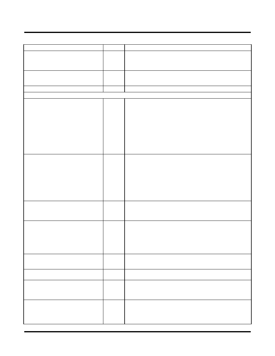
Pinout Information
Lattice Semiconductor
LatticeSC/M Family Data Sheet
RESETN
Reset. (Also sent to general routing). During configuration it resets the
configuration state machine. After configuration this pin can perform
the global set/reset (GSR) functions or can be used as a general input
pin.
CFGIRQN
O
MPI Interrupt request active low signal is controlled by system bus
interrupt controller and may be sourced from any bus error or MPI con-
figuration error. It can be connected to one of MPC860 IRQ pins.
TSALLN
I
Tristates all I/O.
Configuration Pads (User I/O if not used. Used during sysCONFIG.)
HDC/SI
O
High During Configuration is output high until configuration is com-
plete. It is used as a control output, indicating that configuration is not
complete.
For SPI modes, this pin is used to download the read command and
initial read address into the Flash memory device on the falling edge of
SCK. This pin will be connected to SI of the memory. If the SPI mode
is used, the 8-bit instruction code 0x03 will be downloaded followed by
a 24-bit starting address of 0x000000 or a non-zero stat address for
partial reconfiguration. If the SPIX mode has been selected, the 8-bit
instruction captured on D[7:0] at power-up will be shifted in and fol-
lowed by a 32-bit starting address of 0x000000.
LDCN/SCS
O
Low During Configuration is output low until configuration is complete.
It is used as a control output, indicating that configuration is not com-
plete.
For SPI modes, this is an active low chip select for Flash memories. It
will go active after INITN goes high but before SCK begins. During
power up LDCN will be low. Once INITN goes high, LDCN will go high
for 100ns-200ns after which time it will go back low and configuration
can begin. During the 100ns-200ns period, the read instruction will be
latched for SPIX mode.
DOUT
O
Serial data output that can drive the D0/DIN of daisy-chained slave
devices. The data-stream from this output will propagate preamble bits
of the bitstream to daisy-chained devices. Data out on DOUT changes
on the rising edge of CCLK.
QOUT/CEON
O
During daisy-chaining configuration, QOUT is the serial data output
that can drive the D0/DIN of daisy-chained slave devices that do not
propagate preamble bits. Data out on QOUT changes on the rising
edge of CCLK.
During parallel-chaining configuration, active low CEON enables the
cascaded slave device to receive bitstream data.
RDN
I
Used in the asynchronous peripheral configuration mode. A low on
RDN changes D[7:3] into status outputs. WRN and RDN should not be
used simultaneously. If they are, the write strobe overrides.
WRN
I
When the FPGA is selected, a low on the write strobe, WRN, loads the
data on D[7:0] inputs into an internal data buffer.
CS0N CS1
I
Used in the asynchronous peripheral, slave parallel and MPI modes.
The FPGA is selected when CS0N is low and CS1 is high. During con-
figuration, a pull-up is enabled on both except with MPI DMA access
control.
A[21:0]
I/O
In master parallel mode, A[21:0] is an output and will address the con-
figuration EPROMs up to 4 MB space. For MPI configuration mode,
A[17:0] will be the MPI address MPI_ADDR[31:14], A[19:18] will be
the transfer size and A[21:20] will be the burst mode and burst in pro-
cess.
Signal Descriptions (Cont.)
Signal Name
I/O
Description
相關(guān)PDF資料 |
PDF描述 |
|---|---|
| LFSC3GA15E-6FN256I | |
| LFSCM3GA40EP1-5FFN1020I | |
| LFXP2-40E-6FN484I | |
| LFXP2-17E-7F484C | |
| LFXP20E-3FN484C | |
相關(guān)代理商/技術(shù)參數(shù) |
參數(shù)描述 |
|---|---|
| LFSCM3GA80EP1-6FCN1704I | 功能描述:FPGA - 現(xiàn)場可編程門陣列 80.1K LUTs 904 I/O MACOSERDES 1.2V -6I RoHS:否 制造商:Altera Corporation 系列:Cyclone V E 柵極數(shù)量: 邏輯塊數(shù)量:943 內(nèi)嵌式塊RAM - EBR:1956 kbit 輸入/輸出端數(shù)量:128 最大工作頻率:800 MHz 工作電源電壓:1.1 V 最大工作溫度:+ 70 C 安裝風(fēng)格:SMD/SMT 封裝 / 箱體:FBGA-256 |
| LFSCM3GA80EP1-6FF1152C | 功能描述:FPGA - 現(xiàn)場可編程門陣列 80.1K LUTs 660 I/O MACO SERDES1.2V -6SP RoHS:否 制造商:Altera Corporation 系列:Cyclone V E 柵極數(shù)量: 邏輯塊數(shù)量:943 內(nèi)嵌式塊RAM - EBR:1956 kbit 輸入/輸出端數(shù)量:128 最大工作頻率:800 MHz 工作電源電壓:1.1 V 最大工作溫度:+ 70 C 安裝風(fēng)格:SMD/SMT 封裝 / 箱體:FBGA-256 |
| LFSCM3GA80EP1-6FF1152I | 功能描述:FPGA - 現(xiàn)場可編程門陣列 80.1K LUTs 660 I/O MACO SERDES1.2V -6SP RoHS:否 制造商:Altera Corporation 系列:Cyclone V E 柵極數(shù)量: 邏輯塊數(shù)量:943 內(nèi)嵌式塊RAM - EBR:1956 kbit 輸入/輸出端數(shù)量:128 最大工作頻率:800 MHz 工作電源電壓:1.1 V 最大工作溫度:+ 70 C 安裝風(fēng)格:SMD/SMT 封裝 / 箱體:FBGA-256 |
| LFSCM3GA80EP1-6FF1704C | 功能描述:FPGA - 現(xiàn)場可編程門陣列 80.1K LUTs 904 I/O MACO SERDES1.2V -6SP RoHS:否 制造商:Altera Corporation 系列:Cyclone V E 柵極數(shù)量: 邏輯塊數(shù)量:943 內(nèi)嵌式塊RAM - EBR:1956 kbit 輸入/輸出端數(shù)量:128 最大工作頻率:800 MHz 工作電源電壓:1.1 V 最大工作溫度:+ 70 C 安裝風(fēng)格:SMD/SMT 封裝 / 箱體:FBGA-256 |
| LFSCM3GA80EP1-6FF1704I | 功能描述:FPGA - 現(xiàn)場可編程門陣列 80.1K LUTs 904 I/O MACO SERDES1.2V -6SP RoHS:否 制造商:Altera Corporation 系列:Cyclone V E 柵極數(shù)量: 邏輯塊數(shù)量:943 內(nèi)嵌式塊RAM - EBR:1956 kbit 輸入/輸出端數(shù)量:128 最大工作頻率:800 MHz 工作電源電壓:1.1 V 最大工作溫度:+ 70 C 安裝風(fēng)格:SMD/SMT 封裝 / 箱體:FBGA-256 |
發(fā)布緊急采購,3分鐘左右您將得到回復(fù)。