- 您現(xiàn)在的位置:買(mǎi)賣(mài)IC網(wǎng) > PDF目錄299403 > LFSCM3GA80EP1-6FCN1704C (LATTICE SEMICONDUCTOR CORP) PDF資料下載
參數(shù)資料
| 型號(hào): | LFSCM3GA80EP1-6FCN1704C |
| 廠商: | LATTICE SEMICONDUCTOR CORP |
| 元件分類: | FPGA |
| 中文描述: | FPGA, 308 CLBS, 80000 GATES, 1000 MHz, CBGA1704 |
| 封裝: | 42.5 X 42.5 MM, LEAD FREE, CERAMIC, FCBGA-1704 |
| 文件頁(yè)數(shù): | 135/243頁(yè) |
| 文件大?。?/td> | 2674K |
| 代理商: | LFSCM3GA80EP1-6FCN1704C |
第1頁(yè)第2頁(yè)第3頁(yè)第4頁(yè)第5頁(yè)第6頁(yè)第7頁(yè)第8頁(yè)第9頁(yè)第10頁(yè)第11頁(yè)第12頁(yè)第13頁(yè)第14頁(yè)第15頁(yè)第16頁(yè)第17頁(yè)第18頁(yè)第19頁(yè)第20頁(yè)第21頁(yè)第22頁(yè)第23頁(yè)第24頁(yè)第25頁(yè)第26頁(yè)第27頁(yè)第28頁(yè)第29頁(yè)第30頁(yè)第31頁(yè)第32頁(yè)第33頁(yè)第34頁(yè)第35頁(yè)第36頁(yè)第37頁(yè)第38頁(yè)第39頁(yè)第40頁(yè)第41頁(yè)第42頁(yè)第43頁(yè)第44頁(yè)第45頁(yè)第46頁(yè)第47頁(yè)第48頁(yè)第49頁(yè)第50頁(yè)第51頁(yè)第52頁(yè)第53頁(yè)第54頁(yè)第55頁(yè)第56頁(yè)第57頁(yè)第58頁(yè)第59頁(yè)第60頁(yè)第61頁(yè)第62頁(yè)第63頁(yè)第64頁(yè)第65頁(yè)第66頁(yè)第67頁(yè)第68頁(yè)第69頁(yè)第70頁(yè)第71頁(yè)第72頁(yè)第73頁(yè)第74頁(yè)第75頁(yè)第76頁(yè)第77頁(yè)第78頁(yè)第79頁(yè)第80頁(yè)第81頁(yè)第82頁(yè)第83頁(yè)第84頁(yè)第85頁(yè)第86頁(yè)第87頁(yè)第88頁(yè)第89頁(yè)第90頁(yè)第91頁(yè)第92頁(yè)第93頁(yè)第94頁(yè)第95頁(yè)第96頁(yè)第97頁(yè)第98頁(yè)第99頁(yè)第100頁(yè)第101頁(yè)第102頁(yè)第103頁(yè)第104頁(yè)第105頁(yè)第106頁(yè)第107頁(yè)第108頁(yè)第109頁(yè)第110頁(yè)第111頁(yè)第112頁(yè)第113頁(yè)第114頁(yè)第115頁(yè)第116頁(yè)第117頁(yè)第118頁(yè)第119頁(yè)第120頁(yè)第121頁(yè)第122頁(yè)第123頁(yè)第124頁(yè)第125頁(yè)第126頁(yè)第127頁(yè)第128頁(yè)第129頁(yè)第130頁(yè)第131頁(yè)第132頁(yè)第133頁(yè)第134頁(yè)當(dāng)前第135頁(yè)第136頁(yè)第137頁(yè)第138頁(yè)第139頁(yè)第140頁(yè)第141頁(yè)第142頁(yè)第143頁(yè)第144頁(yè)第145頁(yè)第146頁(yè)第147頁(yè)第148頁(yè)第149頁(yè)第150頁(yè)第151頁(yè)第152頁(yè)第153頁(yè)第154頁(yè)第155頁(yè)第156頁(yè)第157頁(yè)第158頁(yè)第159頁(yè)第160頁(yè)第161頁(yè)第162頁(yè)第163頁(yè)第164頁(yè)第165頁(yè)第166頁(yè)第167頁(yè)第168頁(yè)第169頁(yè)第170頁(yè)第171頁(yè)第172頁(yè)第173頁(yè)第174頁(yè)第175頁(yè)第176頁(yè)第177頁(yè)第178頁(yè)第179頁(yè)第180頁(yè)第181頁(yè)第182頁(yè)第183頁(yè)第184頁(yè)第185頁(yè)第186頁(yè)第187頁(yè)第188頁(yè)第189頁(yè)第190頁(yè)第191頁(yè)第192頁(yè)第193頁(yè)第194頁(yè)第195頁(yè)第196頁(yè)第197頁(yè)第198頁(yè)第199頁(yè)第200頁(yè)第201頁(yè)第202頁(yè)第203頁(yè)第204頁(yè)第205頁(yè)第206頁(yè)第207頁(yè)第208頁(yè)第209頁(yè)第210頁(yè)第211頁(yè)第212頁(yè)第213頁(yè)第214頁(yè)第215頁(yè)第216頁(yè)第217頁(yè)第218頁(yè)第219頁(yè)第220頁(yè)第221頁(yè)第222頁(yè)第223頁(yè)第224頁(yè)第225頁(yè)第226頁(yè)第227頁(yè)第228頁(yè)第229頁(yè)第230頁(yè)第231頁(yè)第232頁(yè)第233頁(yè)第234頁(yè)第235頁(yè)第236頁(yè)第237頁(yè)第238頁(yè)第239頁(yè)第240頁(yè)第241頁(yè)第242頁(yè)第243頁(yè)
2-18
Architecture
Lattice Semiconductor
LatticeSC/M Family Data Sheet
Adaptive Input Logic (AIL) Overview
The Adaptive Input Logic (AIL) provides the ability of the input logic to dynamically find a solution by monitoring
multiple samples of the input data. The input data signal from the input buffer is run through a delay chain. Data,
transitions, jitter, noise are all contained inside of the delay chain. The AIL will then search the delay chain for a
clean sampling point for data. Once found the AIL will monitor and walk with the data dynamically. This novel
approach of using a delay chain to create multiple copies of the data provides a lower power solution than overs-
ampling data with a higher speed clock. Figure 2-19 provides a high level view of the AIL methodology.
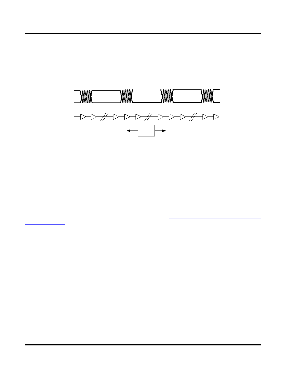
Figure 2-19. LatticeSC AIL Delay of Input Data Waveform
The AIL slides the acquisition window through the delay chain searching for stable data based solely on data tran-
sitions. A specific training pattern is not required to perform this bit alignment, simply data transitions. The size of
the acquisition window is user-selectable allowing the AIL to operate over the full range of the PURESPEED I/O
range. Based on dynamic user control the AIL can either continuously adjust the window location based on data
edge detection or it can be locked to a specific delay.
The AIL operates on single data and double data rate interfaces and is available on most FPGA input pins on the
LatticeSC device and all buffer types. The AIL block is low power using only 0.003 mW/MHz typical (6 mW @ 2
Gbps) for PRBS 2
7 data. Multiple AIL inputs can be used to create a bus with a FPGA circuit to realign the bus to a
common clock cycle. The FPGA circuit to realign the bus is required and is provided by Lattice as a reference
design.
For more information on the LatticeSC AIL please refer to TN1158 LatticeSC PURESPEED I/O Adaptive Input
Input DDR/Shift Block
The DDR/Shift block contains registers and associated logic that support DDR and shift register functions using the
high-speed clock and the associated transfer to the low-speed clock domain. It functions as a gearbox allowing
high-speed incoming data to be passed into the FPGA fabric. Each PIO supports DDR and x2 shift functions. If
desired PIOs A and B or C and D can be combined to form x4 shift functions. The PIOs A and C on the left, right
and bottom of the device also contain an optional Adaptive Input Logic (AIL) element. This logic automatically
aligns incoming data with the clock allowing for easy design of high-speed interfaces. Figure 2-21 shows a simpli-
fied block diagram of the shift register block. The shift block in conjunction with the update and clock divider blocks
automatically handles the hand off between the low-speed and high-speed clock domains.
Delay Chain
Input Data Signal
AIL Acquisition Window
相關(guān)PDF資料 |
PDF描述 |
|---|---|
| LFSC3GA15E-6FN256I | |
| LFSCM3GA40EP1-5FFN1020I | |
| LFXP2-40E-6FN484I | |
| LFXP2-17E-7F484C | |
| LFXP20E-3FN484C | |
相關(guān)代理商/技術(shù)參數(shù) |
參數(shù)描述 |
|---|---|
| LFSCM3GA80EP1-6FCN1704I | 功能描述:FPGA - 現(xiàn)場(chǎng)可編程門(mén)陣列 80.1K LUTs 904 I/O MACOSERDES 1.2V -6I RoHS:否 制造商:Altera Corporation 系列:Cyclone V E 柵極數(shù)量: 邏輯塊數(shù)量:943 內(nèi)嵌式塊RAM - EBR:1956 kbit 輸入/輸出端數(shù)量:128 最大工作頻率:800 MHz 工作電源電壓:1.1 V 最大工作溫度:+ 70 C 安裝風(fēng)格:SMD/SMT 封裝 / 箱體:FBGA-256 |
| LFSCM3GA80EP1-6FF1152C | 功能描述:FPGA - 現(xiàn)場(chǎng)可編程門(mén)陣列 80.1K LUTs 660 I/O MACO SERDES1.2V -6SP RoHS:否 制造商:Altera Corporation 系列:Cyclone V E 柵極數(shù)量: 邏輯塊數(shù)量:943 內(nèi)嵌式塊RAM - EBR:1956 kbit 輸入/輸出端數(shù)量:128 最大工作頻率:800 MHz 工作電源電壓:1.1 V 最大工作溫度:+ 70 C 安裝風(fēng)格:SMD/SMT 封裝 / 箱體:FBGA-256 |
| LFSCM3GA80EP1-6FF1152I | 功能描述:FPGA - 現(xiàn)場(chǎng)可編程門(mén)陣列 80.1K LUTs 660 I/O MACO SERDES1.2V -6SP RoHS:否 制造商:Altera Corporation 系列:Cyclone V E 柵極數(shù)量: 邏輯塊數(shù)量:943 內(nèi)嵌式塊RAM - EBR:1956 kbit 輸入/輸出端數(shù)量:128 最大工作頻率:800 MHz 工作電源電壓:1.1 V 最大工作溫度:+ 70 C 安裝風(fēng)格:SMD/SMT 封裝 / 箱體:FBGA-256 |
| LFSCM3GA80EP1-6FF1704C | 功能描述:FPGA - 現(xiàn)場(chǎng)可編程門(mén)陣列 80.1K LUTs 904 I/O MACO SERDES1.2V -6SP RoHS:否 制造商:Altera Corporation 系列:Cyclone V E 柵極數(shù)量: 邏輯塊數(shù)量:943 內(nèi)嵌式塊RAM - EBR:1956 kbit 輸入/輸出端數(shù)量:128 最大工作頻率:800 MHz 工作電源電壓:1.1 V 最大工作溫度:+ 70 C 安裝風(fēng)格:SMD/SMT 封裝 / 箱體:FBGA-256 |
| LFSCM3GA80EP1-6FF1704I | 功能描述:FPGA - 現(xiàn)場(chǎng)可編程門(mén)陣列 80.1K LUTs 904 I/O MACO SERDES1.2V -6SP RoHS:否 制造商:Altera Corporation 系列:Cyclone V E 柵極數(shù)量: 邏輯塊數(shù)量:943 內(nèi)嵌式塊RAM - EBR:1956 kbit 輸入/輸出端數(shù)量:128 最大工作頻率:800 MHz 工作電源電壓:1.1 V 最大工作溫度:+ 70 C 安裝風(fēng)格:SMD/SMT 封裝 / 箱體:FBGA-256 |
發(fā)布緊急采購(gòu),3分鐘左右您將得到回復(fù)。