- 您現(xiàn)在的位置:買賣IC網(wǎng) > PDF目錄299403 > LFSCM3GA40EP1-5FFN1020I (LATTICE SEMICONDUCTOR CORP) PDF資料下載
參數(shù)資料
| 型號: | LFSCM3GA40EP1-5FFN1020I |
| 廠商: | LATTICE SEMICONDUCTOR CORP |
| 元件分類: | FPGA |
| 中文描述: | FPGA, 216 CLBS, 40000 GATES, 1000 MHz, PBGA1020 |
| 封裝: | 33 X 33 MM, LEAD FREE, FCBGA-1020 |
| 文件頁數(shù): | 180/243頁 |
| 文件大小: | 2674K |
| 代理商: | LFSCM3GA40EP1-5FFN1020I |
第1頁第2頁第3頁第4頁第5頁第6頁第7頁第8頁第9頁第10頁第11頁第12頁第13頁第14頁第15頁第16頁第17頁第18頁第19頁第20頁第21頁第22頁第23頁第24頁第25頁第26頁第27頁第28頁第29頁第30頁第31頁第32頁第33頁第34頁第35頁第36頁第37頁第38頁第39頁第40頁第41頁第42頁第43頁第44頁第45頁第46頁第47頁第48頁第49頁第50頁第51頁第52頁第53頁第54頁第55頁第56頁第57頁第58頁第59頁第60頁第61頁第62頁第63頁第64頁第65頁第66頁第67頁第68頁第69頁第70頁第71頁第72頁第73頁第74頁第75頁第76頁第77頁第78頁第79頁第80頁第81頁第82頁第83頁第84頁第85頁第86頁第87頁第88頁第89頁第90頁第91頁第92頁第93頁第94頁第95頁第96頁第97頁第98頁第99頁第100頁第101頁第102頁第103頁第104頁第105頁第106頁第107頁第108頁第109頁第110頁第111頁第112頁第113頁第114頁第115頁第116頁第117頁第118頁第119頁第120頁第121頁第122頁第123頁第124頁第125頁第126頁第127頁第128頁第129頁第130頁第131頁第132頁第133頁第134頁第135頁第136頁第137頁第138頁第139頁第140頁第141頁第142頁第143頁第144頁第145頁第146頁第147頁第148頁第149頁第150頁第151頁第152頁第153頁第154頁第155頁第156頁第157頁第158頁第159頁第160頁第161頁第162頁第163頁第164頁第165頁第166頁第167頁第168頁第169頁第170頁第171頁第172頁第173頁第174頁第175頁第176頁第177頁第178頁第179頁當前第180頁第181頁第182頁第183頁第184頁第185頁第186頁第187頁第188頁第189頁第190頁第191頁第192頁第193頁第194頁第195頁第196頁第197頁第198頁第199頁第200頁第201頁第202頁第203頁第204頁第205頁第206頁第207頁第208頁第209頁第210頁第211頁第212頁第213頁第214頁第215頁第216頁第217頁第218頁第219頁第220頁第221頁第222頁第223頁第224頁第225頁第226頁第227頁第228頁第229頁第230頁第231頁第232頁第233頁第234頁第235頁第236頁第237頁第238頁第239頁第240頁第241頁第242頁第243頁
2-37
Architecture
Lattice Semiconductor
LatticeSC/M Family Data Sheet
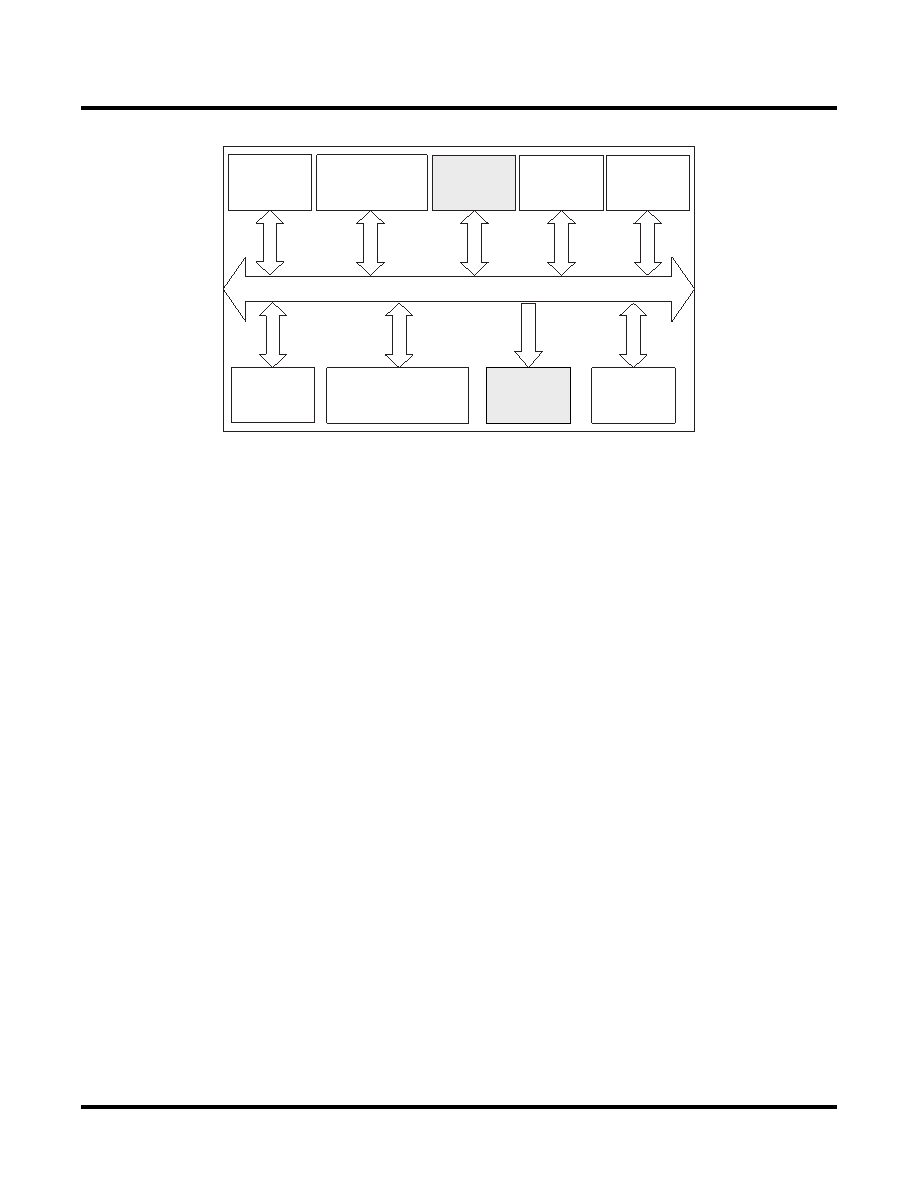
Figure 2-31. LatticeSC System Bus Interfaces
Several interfaces exist between the System Bus and other FPGA elements. The MPI interface acts as a bridge
between the external microprocessor bus and System Bus. The MPI may work in an independent clock domain
from the System Bus if the System Bus clock is not sourced from the external microprocessor clock. Pipelined
operation allows high-speed memory interface to the EBR and peripheral access without the requirement for addi-
tional cycles on the bus. Burst transfers allow optimal use of the memory interface by giving advance information of
the nature of the transfers.
Details for the majority of the peripherals can be found in the associated technical documentation, see details at
the end of this data sheet. Additional details of the MPI are provided below.
Microprocessor Interface (MPI)
The LatticeSC family devices have a dedicated synchronous MPI function block. The MPI is programmable to oper-
ate with PowerPC/PowerQUICC MPC860/MPC8260 series microprocessors. The MPI implements an 8-, 16-, or
32-bit interface with 1-bit, 2-bit, or 4-bit parity to the host processor (PowerPC) that can be used for configuration
and read-back of the FPGA as well as for user-defined data processing and general monitoring of FPGA functions.
The control portion of the MPI is available following power-up of the FPGA if the mode pins specify MPI mode, even
if the FPGA is not yet configured. The width of the data port is selectable among 8-, 16-, or 32-bit and the parity bus
can be 1-, 2-, or 4-bit. In configuration mode the data and parity bus width are related to the state of the M[0:3]
mode pins. For post-configuration use, the MPI must be included in the configuration bit stream by using an MPI
library element in your design from the ispLEVER primitive library, or by setting the bit of the MPI configuration con-
trol register prior to the start of configuration. The user can also enable and disable the parity bus through the con-
figuration bit stream. These pads can be used as general I/O when they are not needed for MPI use.
The MPI block also provides the capability to interface directly to the FPGA fabric with a databus after configura-
tion.The bus protocol is still handled by the MPI block but the direct FPGA access allows high-speed block data
transfers such as DMA transactions. Figure 2-32 shows one of the ways a PowerPC is connected to MPI.
DFA
(Direct Access
from MPI)
SMI
(PLL, DLL,
USER LOGIC)
STATUS and
CONFIG
(SYS REG)
CONFIG
(MASTER)
System Bus
USI
(SLAVE)
UMI
(MASTER)
EBR INIT
(WRITE)
MPI
(MASTER)
PCS (LEFT, RIGHT
and INTER-QUAD)
(SLAVE)
相關(guān)PDF資料 |
PDF描述 |
|---|---|
| LFXP2-40E-6FN484I | |
| LFXP2-17E-7F484C | |
| LFXP20E-3FN484C | |
| LFXP20E-5FN484C | |
| LFXP15C-4FN256C | |
相關(guān)代理商/技術(shù)參數(shù) |
參數(shù)描述 |
|---|---|
| LFSCM3GA40EP1-5FFN1152C | 功能描述:FPGA - 現(xiàn)場可編程門陣列 40.4K LUTs 604 I/O MACO SERDES1.2V -5SP RoHS:否 制造商:Altera Corporation 系列:Cyclone V E 柵極數(shù)量: 邏輯塊數(shù)量:943 內(nèi)嵌式塊RAM - EBR:1956 kbit 輸入/輸出端數(shù)量:128 最大工作頻率:800 MHz 工作電源電壓:1.1 V 最大工作溫度:+ 70 C 安裝風格:SMD/SMT 封裝 / 箱體:FBGA-256 |
| LFSCM3GA40EP1-5FFN1152I | 功能描述:FPGA - 現(xiàn)場可編程門陣列 40.4K LUTs 604 I/O MACO SERDES1.2V -5SP RoHS:否 制造商:Altera Corporation 系列:Cyclone V E 柵極數(shù)量: 邏輯塊數(shù)量:943 內(nèi)嵌式塊RAM - EBR:1956 kbit 輸入/輸出端數(shù)量:128 最大工作頻率:800 MHz 工作電源電壓:1.1 V 最大工作溫度:+ 70 C 安裝風格:SMD/SMT 封裝 / 箱體:FBGA-256 |
| LFSCM3GA40EP1-6FC1152C | 功能描述:FPGA - 現(xiàn)場可編程門陣列 40.4K LUTs 604 I/O MACO SERDES 1.2V -6 RoHS:否 制造商:Altera Corporation 系列:Cyclone V E 柵極數(shù)量: 邏輯塊數(shù)量:943 內(nèi)嵌式塊RAM - EBR:1956 kbit 輸入/輸出端數(shù)量:128 最大工作頻率:800 MHz 工作電源電壓:1.1 V 最大工作溫度:+ 70 C 安裝風格:SMD/SMT 封裝 / 箱體:FBGA-256 |
| LFSCM3GA40EP1-6FC1152I | 功能描述:FPGA - 現(xiàn)場可編程門陣列 40.4K LUTs 604 I/O MACO SERDES 1.2V -6I RoHS:否 制造商:Altera Corporation 系列:Cyclone V E 柵極數(shù)量: 邏輯塊數(shù)量:943 內(nèi)嵌式塊RAM - EBR:1956 kbit 輸入/輸出端數(shù)量:128 最大工作頻率:800 MHz 工作電源電壓:1.1 V 最大工作溫度:+ 70 C 安裝風格:SMD/SMT 封裝 / 箱體:FBGA-256 |
| LFSCM3GA40EP1-6FCN1152C | 功能描述:FPGA - 現(xiàn)場可編程門陣列 40.4K LUTs 604 I/O MACO SERDES 1.2V -6 RoHS:否 制造商:Altera Corporation 系列:Cyclone V E 柵極數(shù)量: 邏輯塊數(shù)量:943 內(nèi)嵌式塊RAM - EBR:1956 kbit 輸入/輸出端數(shù)量:128 最大工作頻率:800 MHz 工作電源電壓:1.1 V 最大工作溫度:+ 70 C 安裝風格:SMD/SMT 封裝 / 箱體:FBGA-256 |
發(fā)布緊急采購,3分鐘左右您將得到回復(fù)。