- 您現(xiàn)在的位置:買賣IC網(wǎng) > PDF目錄299403 > LFSCM3GA40EP1-5FFN1020I (LATTICE SEMICONDUCTOR CORP) PDF資料下載
參數(shù)資料
| 型號: | LFSCM3GA40EP1-5FFN1020I |
| 廠商: | LATTICE SEMICONDUCTOR CORP |
| 元件分類: | FPGA |
| 中文描述: | FPGA, 216 CLBS, 40000 GATES, 1000 MHz, PBGA1020 |
| 封裝: | 33 X 33 MM, LEAD FREE, FCBGA-1020 |
| 文件頁數(shù): | 176/243頁 |
| 文件大小: | 2674K |
| 代理商: | LFSCM3GA40EP1-5FFN1020I |
第1頁第2頁第3頁第4頁第5頁第6頁第7頁第8頁第9頁第10頁第11頁第12頁第13頁第14頁第15頁第16頁第17頁第18頁第19頁第20頁第21頁第22頁第23頁第24頁第25頁第26頁第27頁第28頁第29頁第30頁第31頁第32頁第33頁第34頁第35頁第36頁第37頁第38頁第39頁第40頁第41頁第42頁第43頁第44頁第45頁第46頁第47頁第48頁第49頁第50頁第51頁第52頁第53頁第54頁第55頁第56頁第57頁第58頁第59頁第60頁第61頁第62頁第63頁第64頁第65頁第66頁第67頁第68頁第69頁第70頁第71頁第72頁第73頁第74頁第75頁第76頁第77頁第78頁第79頁第80頁第81頁第82頁第83頁第84頁第85頁第86頁第87頁第88頁第89頁第90頁第91頁第92頁第93頁第94頁第95頁第96頁第97頁第98頁第99頁第100頁第101頁第102頁第103頁第104頁第105頁第106頁第107頁第108頁第109頁第110頁第111頁第112頁第113頁第114頁第115頁第116頁第117頁第118頁第119頁第120頁第121頁第122頁第123頁第124頁第125頁第126頁第127頁第128頁第129頁第130頁第131頁第132頁第133頁第134頁第135頁第136頁第137頁第138頁第139頁第140頁第141頁第142頁第143頁第144頁第145頁第146頁第147頁第148頁第149頁第150頁第151頁第152頁第153頁第154頁第155頁第156頁第157頁第158頁第159頁第160頁第161頁第162頁第163頁第164頁第165頁第166頁第167頁第168頁第169頁第170頁第171頁第172頁第173頁第174頁第175頁當前第176頁第177頁第178頁第179頁第180頁第181頁第182頁第183頁第184頁第185頁第186頁第187頁第188頁第189頁第190頁第191頁第192頁第193頁第194頁第195頁第196頁第197頁第198頁第199頁第200頁第201頁第202頁第203頁第204頁第205頁第206頁第207頁第208頁第209頁第210頁第211頁第212頁第213頁第214頁第215頁第216頁第217頁第218頁第219頁第220頁第221頁第222頁第223頁第224頁第225頁第226頁第227頁第228頁第229頁第230頁第231頁第232頁第233頁第234頁第235頁第236頁第237頁第238頁第239頁第240頁第241頁第242頁第243頁
2-34
Architecture
Lattice Semiconductor
LatticeSC/M Family Data Sheet
VDDAX25 needs to be connected independent of the use of the SERDES. This supply is used to control the
SERDES CML I/O regardless of the SERDES being used in the design.
Supported Source Synchronous Interfaces
The LatticeSC devices contain a variety of hardware, such as delay elements, DDR registers and PLLs, to simplify
the implementation of Source Synchronous interfaces. Table 2-11 lists Source Synchronous and DDR/QDR stan-
dards supported in the LatticeSC. For additional detail refer to technical information at the end of the data sheet.
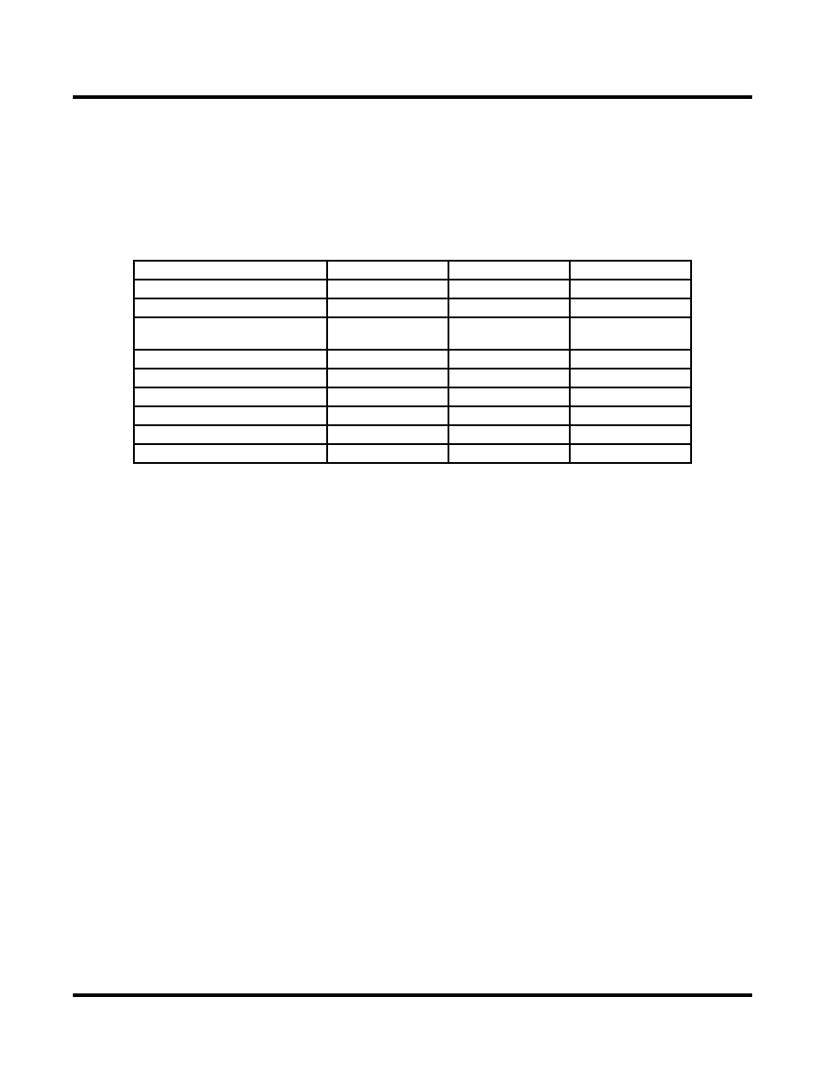
Table 2-11. Source Synchronous Standards Table
1
flexiPCS (Physical Coding Sublayer Block)
flexiPCS Functionality
The LatticeSC family combines a high-performance FPGA fabric, high-performance I/Os and large embedded
RAM in a single industry leading architecture. LatticeSC devices also feature up to 32 channels of embedded
SERDES with associated Physical Coding Sublayer (PCS) logic. The flexiPCS logic can be configured to support
numerous industry standard high-speed data transfer protocols.
Each channel of flexiPCS logic contains dedicated transmit and receive SERDES for high-speed, full-duplex serial
data transfers at data rates up to 3.8 Gbps. The PCS logic in each channel can be configured to support an array of
popular data protocols including SONET (STS-12/STS-12c, STS-48/STS-48c, and TFI-5 support of 10 Gbps or
above), Gigabit Ethernet (compliant to the IEEE 1000BASE-X specification), 1.02 or 2.04 Gbps Fibre Channel,
PCI-Express, and Serial RapidIO. In addition, the protocol based logic can be fully or partially bypassed in a num-
ber of configurations to allow users flexibility in designing their own high-speed data interface.
Protocols requiring data rates above 3.8 Gbps can be accommodated by dedicating either one pair or all four chan-
nels in one flexiPCS quad block to one data link. One quad can support full-duplex serial data transfers at data
rates up to 15.2 Gbps. A single flexiPCS quad can be configured to support 10Gb Ethernet (with a fully compliant
XAUI interface), 10Gb Fibre Channel, and x4 PCI-Express and 4x RapidIO.
The flexiPCS also provides bypass modes that allow a direct 8-bit or 10-bit interface from the SERDES to the
FPGA logic which can also be geared to run at 1/2 speed for a 16-bit or 20-bit interface to the FPGA logic. Each
SERDES pin can be DC coupled independently and can allow for both high-speed and low-speed operation down
to DC rates on the same SERDES pin, as required by some Serial Digital Video applications.
The ispLEVER design tools from Lattice support all modes of the flexiPCS. Most modes are dedicated to applica-
tions associated with a specific industry standard data protocol. Other more general purpose modes allow a user to
define their own operation. With ispLEVER, the user can define the mode for each quad in a design. Nine modes
are currently supported by the ispLEVER design flow:
Source Synchronous Standard
Clocking
Speeds (MHz)
Data Rate (Mbps)
RapidIO
DDR
500
1000
SPI4.2 (POS-PHY4)/NPSI
DDR
500
1000
SFI4/XSBI
DDR
SDR
334
667
XGMII
DDR
156.25
312
CSIX
SDR
250
QDRII/QDRII+ memory interface
DDR
300
600
DDR memory interface
DDR
240
480
DDRII memory interface
DDR
333
667
RLDRAM memory interface
DDR
400
800
1. Memory width is dependent on the system design and limited by the number of I/Os in the device.
相關PDF資料 |
PDF描述 |
|---|---|
| LFXP2-40E-6FN484I | |
| LFXP2-17E-7F484C | |
| LFXP20E-3FN484C | |
| LFXP20E-5FN484C | |
| LFXP15C-4FN256C | |
相關代理商/技術參數(shù) |
參數(shù)描述 |
|---|---|
| LFSCM3GA40EP1-5FFN1152C | 功能描述:FPGA - 現(xiàn)場可編程門陣列 40.4K LUTs 604 I/O MACO SERDES1.2V -5SP RoHS:否 制造商:Altera Corporation 系列:Cyclone V E 柵極數(shù)量: 邏輯塊數(shù)量:943 內嵌式塊RAM - EBR:1956 kbit 輸入/輸出端數(shù)量:128 最大工作頻率:800 MHz 工作電源電壓:1.1 V 最大工作溫度:+ 70 C 安裝風格:SMD/SMT 封裝 / 箱體:FBGA-256 |
| LFSCM3GA40EP1-5FFN1152I | 功能描述:FPGA - 現(xiàn)場可編程門陣列 40.4K LUTs 604 I/O MACO SERDES1.2V -5SP RoHS:否 制造商:Altera Corporation 系列:Cyclone V E 柵極數(shù)量: 邏輯塊數(shù)量:943 內嵌式塊RAM - EBR:1956 kbit 輸入/輸出端數(shù)量:128 最大工作頻率:800 MHz 工作電源電壓:1.1 V 最大工作溫度:+ 70 C 安裝風格:SMD/SMT 封裝 / 箱體:FBGA-256 |
| LFSCM3GA40EP1-6FC1152C | 功能描述:FPGA - 現(xiàn)場可編程門陣列 40.4K LUTs 604 I/O MACO SERDES 1.2V -6 RoHS:否 制造商:Altera Corporation 系列:Cyclone V E 柵極數(shù)量: 邏輯塊數(shù)量:943 內嵌式塊RAM - EBR:1956 kbit 輸入/輸出端數(shù)量:128 最大工作頻率:800 MHz 工作電源電壓:1.1 V 最大工作溫度:+ 70 C 安裝風格:SMD/SMT 封裝 / 箱體:FBGA-256 |
| LFSCM3GA40EP1-6FC1152I | 功能描述:FPGA - 現(xiàn)場可編程門陣列 40.4K LUTs 604 I/O MACO SERDES 1.2V -6I RoHS:否 制造商:Altera Corporation 系列:Cyclone V E 柵極數(shù)量: 邏輯塊數(shù)量:943 內嵌式塊RAM - EBR:1956 kbit 輸入/輸出端數(shù)量:128 最大工作頻率:800 MHz 工作電源電壓:1.1 V 最大工作溫度:+ 70 C 安裝風格:SMD/SMT 封裝 / 箱體:FBGA-256 |
| LFSCM3GA40EP1-6FCN1152C | 功能描述:FPGA - 現(xiàn)場可編程門陣列 40.4K LUTs 604 I/O MACO SERDES 1.2V -6 RoHS:否 制造商:Altera Corporation 系列:Cyclone V E 柵極數(shù)量: 邏輯塊數(shù)量:943 內嵌式塊RAM - EBR:1956 kbit 輸入/輸出端數(shù)量:128 最大工作頻率:800 MHz 工作電源電壓:1.1 V 最大工作溫度:+ 70 C 安裝風格:SMD/SMT 封裝 / 箱體:FBGA-256 |
發(fā)布緊急采購,3分鐘左右您將得到回復。