- 您現(xiàn)在的位置:買賣IC網(wǎng) > PDF目錄299403 > LFSCM3GA40EP1-5FFN1020I (LATTICE SEMICONDUCTOR CORP) PDF資料下載
參數(shù)資料
| 型號(hào): | LFSCM3GA40EP1-5FFN1020I |
| 廠商: | LATTICE SEMICONDUCTOR CORP |
| 元件分類: | FPGA |
| 中文描述: | FPGA, 216 CLBS, 40000 GATES, 1000 MHz, PBGA1020 |
| 封裝: | 33 X 33 MM, LEAD FREE, FCBGA-1020 |
| 文件頁(yè)數(shù): | 159/243頁(yè) |
| 文件大?。?/td> | 2674K |
| 代理商: | LFSCM3GA40EP1-5FFN1020I |
第1頁(yè)第2頁(yè)第3頁(yè)第4頁(yè)第5頁(yè)第6頁(yè)第7頁(yè)第8頁(yè)第9頁(yè)第10頁(yè)第11頁(yè)第12頁(yè)第13頁(yè)第14頁(yè)第15頁(yè)第16頁(yè)第17頁(yè)第18頁(yè)第19頁(yè)第20頁(yè)第21頁(yè)第22頁(yè)第23頁(yè)第24頁(yè)第25頁(yè)第26頁(yè)第27頁(yè)第28頁(yè)第29頁(yè)第30頁(yè)第31頁(yè)第32頁(yè)第33頁(yè)第34頁(yè)第35頁(yè)第36頁(yè)第37頁(yè)第38頁(yè)第39頁(yè)第40頁(yè)第41頁(yè)第42頁(yè)第43頁(yè)第44頁(yè)第45頁(yè)第46頁(yè)第47頁(yè)第48頁(yè)第49頁(yè)第50頁(yè)第51頁(yè)第52頁(yè)第53頁(yè)第54頁(yè)第55頁(yè)第56頁(yè)第57頁(yè)第58頁(yè)第59頁(yè)第60頁(yè)第61頁(yè)第62頁(yè)第63頁(yè)第64頁(yè)第65頁(yè)第66頁(yè)第67頁(yè)第68頁(yè)第69頁(yè)第70頁(yè)第71頁(yè)第72頁(yè)第73頁(yè)第74頁(yè)第75頁(yè)第76頁(yè)第77頁(yè)第78頁(yè)第79頁(yè)第80頁(yè)第81頁(yè)第82頁(yè)第83頁(yè)第84頁(yè)第85頁(yè)第86頁(yè)第87頁(yè)第88頁(yè)第89頁(yè)第90頁(yè)第91頁(yè)第92頁(yè)第93頁(yè)第94頁(yè)第95頁(yè)第96頁(yè)第97頁(yè)第98頁(yè)第99頁(yè)第100頁(yè)第101頁(yè)第102頁(yè)第103頁(yè)第104頁(yè)第105頁(yè)第106頁(yè)第107頁(yè)第108頁(yè)第109頁(yè)第110頁(yè)第111頁(yè)第112頁(yè)第113頁(yè)第114頁(yè)第115頁(yè)第116頁(yè)第117頁(yè)第118頁(yè)第119頁(yè)第120頁(yè)第121頁(yè)第122頁(yè)第123頁(yè)第124頁(yè)第125頁(yè)第126頁(yè)第127頁(yè)第128頁(yè)第129頁(yè)第130頁(yè)第131頁(yè)第132頁(yè)第133頁(yè)第134頁(yè)第135頁(yè)第136頁(yè)第137頁(yè)第138頁(yè)第139頁(yè)第140頁(yè)第141頁(yè)第142頁(yè)第143頁(yè)第144頁(yè)第145頁(yè)第146頁(yè)第147頁(yè)第148頁(yè)第149頁(yè)第150頁(yè)第151頁(yè)第152頁(yè)第153頁(yè)第154頁(yè)第155頁(yè)第156頁(yè)第157頁(yè)第158頁(yè)當(dāng)前第159頁(yè)第160頁(yè)第161頁(yè)第162頁(yè)第163頁(yè)第164頁(yè)第165頁(yè)第166頁(yè)第167頁(yè)第168頁(yè)第169頁(yè)第170頁(yè)第171頁(yè)第172頁(yè)第173頁(yè)第174頁(yè)第175頁(yè)第176頁(yè)第177頁(yè)第178頁(yè)第179頁(yè)第180頁(yè)第181頁(yè)第182頁(yè)第183頁(yè)第184頁(yè)第185頁(yè)第186頁(yè)第187頁(yè)第188頁(yè)第189頁(yè)第190頁(yè)第191頁(yè)第192頁(yè)第193頁(yè)第194頁(yè)第195頁(yè)第196頁(yè)第197頁(yè)第198頁(yè)第199頁(yè)第200頁(yè)第201頁(yè)第202頁(yè)第203頁(yè)第204頁(yè)第205頁(yè)第206頁(yè)第207頁(yè)第208頁(yè)第209頁(yè)第210頁(yè)第211頁(yè)第212頁(yè)第213頁(yè)第214頁(yè)第215頁(yè)第216頁(yè)第217頁(yè)第218頁(yè)第219頁(yè)第220頁(yè)第221頁(yè)第222頁(yè)第223頁(yè)第224頁(yè)第225頁(yè)第226頁(yè)第227頁(yè)第228頁(yè)第229頁(yè)第230頁(yè)第231頁(yè)第232頁(yè)第233頁(yè)第234頁(yè)第235頁(yè)第236頁(yè)第237頁(yè)第238頁(yè)第239頁(yè)第240頁(yè)第241頁(yè)第242頁(yè)第243頁(yè)
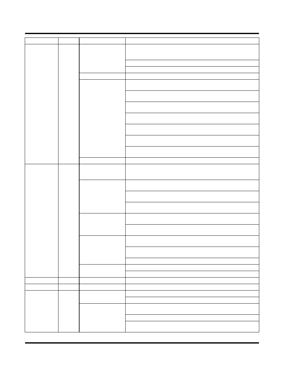
7-3
Revision History
Lattice Semiconductor
LatticeSC/M Family Data Sheet
August 2006
(cont.)
01.3
(cont.)
DC and Switching
Characteristics
(cont.)
Updated LatticeSC Family Timing Adders with ispLEVER 6.0 SP1
results
Updated PLL Timing Parameters based on PDE testing results
Removed RDDATA parameter from sysCONFIG readback timing table
Multiple
Changed TDO/RDDATA to TDO
Pinout Information
Removed all MPI signals from SC15 256 pin package Dual Function
Column
Added note to SC15, SC25 900 pin package that the package supports
a 16 bit MPI
Added note that pin D3 in an SC15 and SC25 900 pin package should
not be used for single-ended outputs
Added note that pin D28 in an SC15 and SC25 900 pin package should
not be used for single-ended outputs
Added note to SC25 1020 pin package that the package supports a 16
bit MPI
Added note to SC80 1152 pin package that the package supports a 32
bit MPI
Added note to SC80 1704 pin package that the package supports a 32
bit MPI
Ordering Information
Changed “fcBGA” for the 1020 packages to “ffBGA”
November 2006
01.4
Introduction
LatticeSC Family Selection Guide table – I/O count for SC80 device,
1704 fcBGA package changed to 904/32. I/O count for SC115 device,
1704 fcBGA package changed to 942/32.
DC and Switching
Characteristics
DC Electrical Characteristics table – Updated the initialization and
standby supply current values.
DC Electrical Characteristics table – Updated the sysCONFIG Master
Parallel mode RCLK low and RCLK high time specifications.
DC Electrical Characteristics table – Updated VCCIO values for
LVPECL33 I/Os.
Pin Information
Pin Information Summary table - Changed number of single ended user
I/Os from 906 to 904 for 1704 fcBGA.
Removed the single-ended only output restriction on pins D3 and D28 in
an SC15 and SC25 900 pin package.
Ordering Information
Ordering Information tables - Changed number of I/Os from 906 to 904
for 1704 fcBGA.
Added ordering part numbers for LatticeSC/SCM 40K and 115K LUT
devices.
Added lead-free ordering part numbers.
Multiple
Changed number of available SC80 I/O from 906 to 904.
Changed number of available SC115 I/O from 944 to 942.
January 2007
01.4a
Architecture
Added EBR Asynchronous Reset section.
February 2007
01.4b
Architecture
Updated EBR Asynchronous Reset section.
March 2007
01.5
Architecture
Added EBR asynchronous reset clarification
Clarified that differential drivers are not supported in banks 1, 4 and 5
DC and Switching
Characteristics
Added clarification for the description of the junction temperature speci-
fication in the Absolute Maximum Ratings section.
Updated Initialization and Standby Current table.
Updated LatticeSC External Switching Characteristics with ispLEVER
6.1 SP1 results.
Date
Version
Section
Change Summary
相關(guān)PDF資料 |
PDF描述 |
|---|---|
| LFXP2-40E-6FN484I | |
| LFXP2-17E-7F484C | |
| LFXP20E-3FN484C | |
| LFXP20E-5FN484C | |
| LFXP15C-4FN256C | |
相關(guān)代理商/技術(shù)參數(shù) |
參數(shù)描述 |
|---|---|
| LFSCM3GA40EP1-5FFN1152C | 功能描述:FPGA - 現(xiàn)場(chǎng)可編程門陣列 40.4K LUTs 604 I/O MACO SERDES1.2V -5SP RoHS:否 制造商:Altera Corporation 系列:Cyclone V E 柵極數(shù)量: 邏輯塊數(shù)量:943 內(nèi)嵌式塊RAM - EBR:1956 kbit 輸入/輸出端數(shù)量:128 最大工作頻率:800 MHz 工作電源電壓:1.1 V 最大工作溫度:+ 70 C 安裝風(fēng)格:SMD/SMT 封裝 / 箱體:FBGA-256 |
| LFSCM3GA40EP1-5FFN1152I | 功能描述:FPGA - 現(xiàn)場(chǎng)可編程門陣列 40.4K LUTs 604 I/O MACO SERDES1.2V -5SP RoHS:否 制造商:Altera Corporation 系列:Cyclone V E 柵極數(shù)量: 邏輯塊數(shù)量:943 內(nèi)嵌式塊RAM - EBR:1956 kbit 輸入/輸出端數(shù)量:128 最大工作頻率:800 MHz 工作電源電壓:1.1 V 最大工作溫度:+ 70 C 安裝風(fēng)格:SMD/SMT 封裝 / 箱體:FBGA-256 |
| LFSCM3GA40EP1-6FC1152C | 功能描述:FPGA - 現(xiàn)場(chǎng)可編程門陣列 40.4K LUTs 604 I/O MACO SERDES 1.2V -6 RoHS:否 制造商:Altera Corporation 系列:Cyclone V E 柵極數(shù)量: 邏輯塊數(shù)量:943 內(nèi)嵌式塊RAM - EBR:1956 kbit 輸入/輸出端數(shù)量:128 最大工作頻率:800 MHz 工作電源電壓:1.1 V 最大工作溫度:+ 70 C 安裝風(fēng)格:SMD/SMT 封裝 / 箱體:FBGA-256 |
| LFSCM3GA40EP1-6FC1152I | 功能描述:FPGA - 現(xiàn)場(chǎng)可編程門陣列 40.4K LUTs 604 I/O MACO SERDES 1.2V -6I RoHS:否 制造商:Altera Corporation 系列:Cyclone V E 柵極數(shù)量: 邏輯塊數(shù)量:943 內(nèi)嵌式塊RAM - EBR:1956 kbit 輸入/輸出端數(shù)量:128 最大工作頻率:800 MHz 工作電源電壓:1.1 V 最大工作溫度:+ 70 C 安裝風(fēng)格:SMD/SMT 封裝 / 箱體:FBGA-256 |
| LFSCM3GA40EP1-6FCN1152C | 功能描述:FPGA - 現(xiàn)場(chǎng)可編程門陣列 40.4K LUTs 604 I/O MACO SERDES 1.2V -6 RoHS:否 制造商:Altera Corporation 系列:Cyclone V E 柵極數(shù)量: 邏輯塊數(shù)量:943 內(nèi)嵌式塊RAM - EBR:1956 kbit 輸入/輸出端數(shù)量:128 最大工作頻率:800 MHz 工作電源電壓:1.1 V 最大工作溫度:+ 70 C 安裝風(fēng)格:SMD/SMT 封裝 / 箱體:FBGA-256 |
發(fā)布緊急采購(gòu),3分鐘左右您將得到回復(fù)。