- 您現(xiàn)在的位置:買賣IC網(wǎng) > PDF目錄383254 > L9352-DIE1 (意法半導(dǎo)體) INTELLIGENT QUAD 2X5A/2X2.5A LOW-SIDE SWITCH PDF資料下載
參數(shù)資料
| 型號(hào): | L9352-DIE1 |
| 廠商: | 意法半導(dǎo)體 |
| 英文描述: | INTELLIGENT QUAD 2X5A/2X2.5A LOW-SIDE SWITCH |
| 中文描述: | 智能四2X5A/2X2.5A低邊開(kāi)關(guān) |
| 文件頁(yè)數(shù): | 4/21頁(yè) |
| 文件大小: | 328K |
| 代理商: | L9352-DIE1 |
第1頁(yè)第2頁(yè)第3頁(yè)當(dāng)前第4頁(yè)第5頁(yè)第6頁(yè)第7頁(yè)第8頁(yè)第9頁(yè)第10頁(yè)第11頁(yè)第12頁(yè)第13頁(yè)第14頁(yè)第15頁(yè)第16頁(yè)第17頁(yè)第18頁(yè)第19頁(yè)第20頁(yè)第21頁(yè)
L9352
4/21
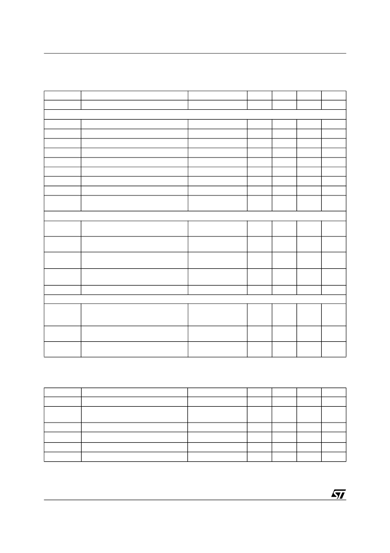
ABSOLUTE MAXIMUM RATINGS
The absolute maximum ratings are the limiting values for this device. Damage may occur if this device is sub-
jected to conditions which are beyond these values.
THERMAL DATA
Symbol
E
Q
Voltages
V
S
V
CC
, V
DD
V
Q
V
Q
V
IN
, V
EN
V
CLK
V
ST
V
D
V
DRmax
Parameter
Test Conditions
Min
Typ
Max
50
Unit
mJ
Switch off energy for inductive loads
Supply voltage
-0.3
40
V
Supply voltage
Output voltage static
Output voltage during clamping
-0.3
6
40
60
V
V
V
t < 1ms
Input voltage IN1 to IN4, EN
Input Voltage CLK
Output voltage status
I
I
< |10|mA
-1.5
-1.5
-0.3
6
6
6
V
V
V
Recirculation circuits D3, D4
max. reverse breakdown voltage of free
wheeling diodes D3, D4
40
55
V
V
Currents
I
Q1/2
Output current for Q1 and Q2
>5
internal
limited
internal
limited
A
I
Q3/4
Output current for Q3 and Q4
>3
A
I
Q1/2
,
I
PGND1/2
I
Q3/4
,
I
PGND3/4
I
ST
ESD Protection
ESD
Output current at reversal supply for Q1
and Q2
-4
A
Output current at reversal supply for
Q3 and Q4
-2
A
Output current status pin
-5
5
mA
Electrostatical Discharging
GND, PGND, Qx, Dx, CLK, ST, IN,
TEST, EN
Supply pins
MIL883C
±
2
kV
VS,
VCC,VDD
ESD
vs. GND and PGND
±1
kV
Output Pins (Qx, Dx)
vs. Common GND
(PGND1-4 + GND)
±
4
kV
Symbol
T
j
T
jc
Parameter
Test Conditions
Min
-40
Typ
Max
150
Unit
°C
Junction temperature
T
j
Σ
t = 30min
Σ
t = 15min
T
stg
Junction temperature during clamping
(life time)
175
190
°C
T
stg
T
th
Storage temperature
Overtemperature shutdown threshold
-55
175
150
200
°C
°C
(1)
(1)
This parameter will not be tested but assured by design
T
hy
R
thJC
Overtemperature shutdown hysteresis
Thermal resistance junction to case
(1)
10
°C
K/W
R
thJC
2
相關(guān)PDF資料 |
PDF描述 |
|---|---|
| L9363 | QUAD INTEGRATED LOW SIDE DRIVER |
| L9377 | DUAL INTELLIGENT POWER LOW SIDE SWITCH |
| L9377DIE1 | DUAL INTELLIGENT POWER LOW SIDE SWITCH |
| L9380 | Triple High-Side MOSFET Driver(三高邊MOSFET驅(qū)動(dòng)器) |
| L9386 | DUAL INTELLIGENT POWER LOW SIDE SWITCH |
相關(guān)代理商/技術(shù)參數(shù) |
參數(shù)描述 |
|---|---|
| L9353M | 制造商:EPCOS 制造商全稱:EPCOS 功能描述:IF Filter for Audio Applications |
| L9355 | 制造商:未知廠家 制造商全稱:未知廠家 功能描述:Dual Peripheral Driver |
| L9360 | 制造商:未知廠家 制造商全稱:未知廠家 功能描述:Injector Driver |
| L9360D | 制造商:未知廠家 制造商全稱:未知廠家 功能描述:Injector Driver |
| L9360M | 制造商:未知廠家 制造商全稱:未知廠家 功能描述:Injector Driver |
發(fā)布緊急采購(gòu),3分鐘左右您將得到回復(fù)。