- 您現(xiàn)在的位置:買賣IC網(wǎng) > PDF目錄384577 > JZ48F4L0QTZ (Intel Corp.) StrataFlash Wireless Memory PDF資料下載
參數(shù)資料
| 型號: | JZ48F4L0QTZ |
| 廠商: | Intel Corp. |
| 英文描述: | StrataFlash Wireless Memory |
| 中文描述: | 無線的StrataFlash存儲器 |
| 文件頁數(shù): | 49/106頁 |
| 文件大小: | 1272K |
| 代理商: | JZ48F4L0QTZ |
第1頁第2頁第3頁第4頁第5頁第6頁第7頁第8頁第9頁第10頁第11頁第12頁第13頁第14頁第15頁第16頁第17頁第18頁第19頁第20頁第21頁第22頁第23頁第24頁第25頁第26頁第27頁第28頁第29頁第30頁第31頁第32頁第33頁第34頁第35頁第36頁第37頁第38頁第39頁第40頁第41頁第42頁第43頁第44頁第45頁第46頁第47頁第48頁當前第49頁第50頁第51頁第52頁第53頁第54頁第55頁第56頁第57頁第58頁第59頁第60頁第61頁第62頁第63頁第64頁第65頁第66頁第67頁第68頁第69頁第70頁第71頁第72頁第73頁第74頁第75頁第76頁第77頁第78頁第79頁第80頁第81頁第82頁第83頁第84頁第85頁第86頁第87頁第88頁第89頁第90頁第91頁第92頁第93頁第94頁第95頁第96頁第97頁第98頁第99頁第100頁第101頁第102頁第103頁第104頁第105頁第106頁
Intel StrataFlash Wireless Memory (L18)
Datasheet
Intel StrataFlash Wireless Memory (L18)
Order Number: 251902, Revision: 009
April 2005
49
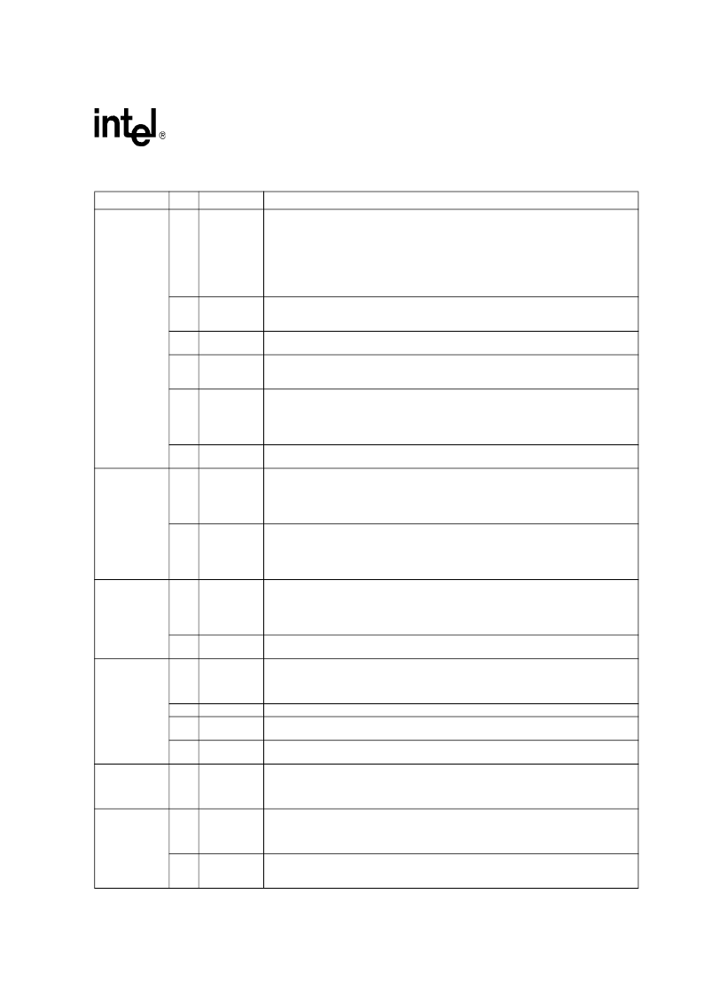
Write
0x40Setup
First cycle of a 2-cycle programming command; prepares the CUI for a write operation.
On the next write cycle, the address and data are latched and the WSM executes the
programming algorithm at the addressed location. During program operations, the
partition responds only to Read Status Register and Program Suspend commands. CE#
or OE# must be toggled to update the Status Register in asynchronous read. CE# or
ADV# must be toggled to update the Status Register Data for synchronous Non-array
read. The Read Array command must be issued to read array data after programming has
finished.
0x10
Alternate Word
Program
Setup
0xE8Program
Buffered
Program
Confirm
Buffered
Enhanced
Factory
Programming
Setup
0xD0Confirm
Equivalent to the Word Program Setup command, 0x40.
This command loads a variable number of bytes up to the buffer size of 32 words onto the
program buffer.
The confirm command is Issued after the data streaming for writing into the buffer is done.
This instructs the WSM to perform the Buffered Program algorithm, writing the data from
the buffer to the flash memory array.
0xD0
0x80
First cycle of a 2-cycle command; initiates Buffered Enhanced Factory Program mode
(Buffered EFP). The CUI then waits for the Buffered EFP Confirm command, 0xD0, that
initiates the Buffered EFP algorithm. All other commands are ignored when Buffered EFP
mode begins.
If the previous command was Buffered EFP Setup (0x80), the CUI latches the address
and data, and prepares the device for Buffered EFP mode.
First cycle of a 2-cycle command; prepares the CUI for a block-erase operation. The
WSM performs the erase algorithm on the block addressed by the Erase Confirm
command. If the next command
is not
the Erase Confirm (0xD0) command, the CUI sets
Status Register bits SR[4] and SR[5], and places the addressed partition in read status
register mode.
If the first command was Block Erase Setup (0x20), the CUI latches the address and data,
and the WSM erases the addressed block. During block-erase operations, the partition
responds only to Read Status Register and Erase Suspend commands. CE# or OE# must
be toggled to update the Status Register in asynchronous read. CE# or ADV# must be
toggled to update the Status Register Data for synchronous Non-array read.
This command issued to any device address initiates a suspend of the currently-
executing program or block erase operation. The Status Register indicates successful
suspend operation by setting either SR[2] (program suspended) or SR[6] (erase
suspended), along with SR[7] (ready). The Write State Machine remains in the suspend
mode regardless of control signal states (except for RST# asserted).
This command issued to any device address resumes the suspended program or block-
erase operation.
First cycle of a 2-cycle command; prepares the CUI for block lock configuration changes.
If the next command is not Block Lock (0x01), Block Unlock (0xD0), or Block Lock-Down
(0x2F), the CUI sets Status Register bits SR[4] and SR[5], indicating a command
sequence error.
If the previous command was Block Lock Setup (0x60), the addressed block is locked.
If the previous command was Block Lock Setup (0x60), the addressed block is unlocked.
If the addressed block is in a lock-down state, the operation has no effect.
If the previous command was Block Lock Setup (0x60), the addressed block is locked
down.
Erase
0x20Setup
0xD0Confirm
Suspend
0xB0
Program or
Erase
Suspend
0xD0Resume
Block Locking/
Unlocking
0x60Setup
0x01 Lock Block
0xD0 Unlock Block
0x2FBlock
Program
Protection
Register
Setup
Read
Configuration
Register
Setup
Read
Configuration
Register
Protection
0xC0
First cycle of a 2-cycle command; prepares the device for a Protection Register or Lock
Register program operation. The second cycle latches the register address and data, and
starts the programming algorithm.
Configuration
0x60
First cycle of a 2-cycle command; prepares the CUI for device read configuration. If the
Set Read Configuration Register command (0x03) is not the next command, the CUI sets
Status Register bits SR[4] and SR[5], indicating a command sequence error.
0x03
If the previous command was Read Configuration Register Setup (0x60), the CUI latches
the address and writes A[15:0] to the Read Configuration Register. Following a Configure
Read Configuration Register command, subsequent read operations access array data.
Table 9.
Command Codes and Definitions (Sheet 2 of 2)
Mode
Code Device Mode
Description
相關PDF資料 |
PDF描述 |
|---|---|
| JZC-32F | SUBMINIATURE INTERMEDIATE POWER RELAY |
| KCA370UH | AM Tuner For Car Audio(汽車音響AM調(diào)諧器) |
| KCC1102A | Electronic AM/FM/MPX/Noise Canceller Tuner(電子式調(diào)幅/調(diào)頻/多路通道噪聲消除器) |
| KCC1202V | Electronic AM/FM/MPX/Noise Canceller Tuner(電子式AM/FM/多路轉換噪聲消除調(diào)諧器) |
| KCF201H | FM Tuner for Car Audio(FM調(diào)諧器(用于汽車音響)) |
相關代理商/技術參數(shù) |
參數(shù)描述 |
|---|---|
| JZ500 | 功能描述:8 ~ 50pF Trimmer Capacitor 110V Top Adjustment Surface Mount 0.177" L x 0.126" W (4.50mm x 3.20mm) 制造商:knowles voltronics 系列:JZ 包裝:剪切帶(CT) 零件狀態(tài):有效 電容范圍:8 ~ 50pF 調(diào)節(jié)類型:頂部調(diào)節(jié) 電壓 - 額定:110V 大小/尺寸:0.177" 長 x 0.126" 寬(4.50mm x 3.20mm) 高度 - 安裝(最大值):0.057"(1.45mm) 安裝類型:表面貼裝 特性:通用 標準包裝:1 |
| JZ58F0046L0Y1G | 制造商:Micron Technology Inc 功能描述:512LCR/256DD 12POP 1.8 X16 HF 128 BALL - Tape and Reel |
| JZ58F0046L0Y1GH0 | 制造商:Micron Technology Inc 功能描述:WIRELESS - Trays |
| JZ58F0046L0Y1GH1 | 制造商:Micron Technology Inc 功能描述:WIRELESS - Tape and Reel |
| JZ58F0046L0Y1GHB | 制造商:Micron Technology Inc 功能描述:WIRELESS - Tape and Reel |
發(fā)布緊急采購,3分鐘左右您將得到回復。