- 您現(xiàn)在的位置:買賣IC網(wǎng) > PDF目錄360742 > ICS1531 Triple 8-bit MSPS A/D Converters with Line-Locked Clock Generator PDF資料下載
參數(shù)資料
| 型號: | ICS1531 |
| 英文描述: | Triple 8-bit MSPS A/D Converters with Line-Locked Clock Generator |
| 中文描述: | 三8位MSPS的的A / D轉換器與電源同步時鐘發(fā)生器 |
| 文件頁數(shù): | 17/76頁 |
| 文件大小: | 529K |
| 代理商: | ICS1531 |
第1頁第2頁第3頁第4頁第5頁第6頁第7頁第8頁第9頁第10頁第11頁第12頁第13頁第14頁第15頁第16頁當前第17頁第18頁第19頁第20頁第21頁第22頁第23頁第24頁第25頁第26頁第27頁第28頁第29頁第30頁第31頁第32頁第33頁第34頁第35頁第36頁第37頁第38頁第39頁第40頁第41頁第42頁第43頁第44頁第45頁第46頁第47頁第48頁第49頁第50頁第51頁第52頁第53頁第54頁第55頁第56頁第57頁第58頁第59頁第60頁第61頁第62頁第63頁第64頁第65頁第66頁第67頁第68頁第69頁第70頁第71頁第72頁第73頁第74頁第75頁第76頁
Chapter 3
Pin Diagram and Listings
ICS1531 Rev N 12/1/99
December, 1999
17
Copyright 1999, Integrated Circuit Systems, Inc.
All rights reserved.
ICS1531 Data Sheet - Preliminary
3.2.3.7
Power Pins
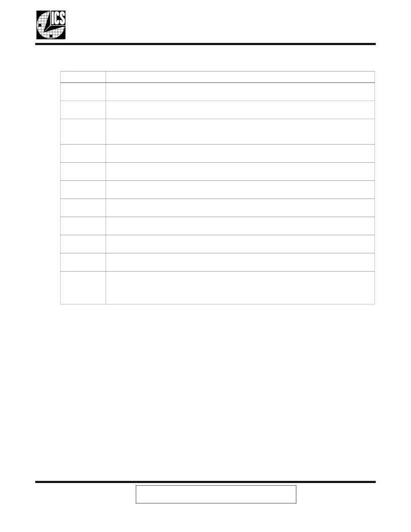
Table 3-9.
Power Pins
Pin Name
Pin Description
VDDA
(3.3 V) Supply for Analog (Pixel PLL Circuitry).
This pin supplies 3.3 V to the analog portions of the pixel PLL circuitry.
VDDAADC
(3.3 V) Supply for Analog ADC (Circuitry).
These pins supply 3.3 V to the analog portions of the ADC.
VDDD
(3.3 V) Supply for Digital (Pixel PLL and Industry-Standard 2-Wire Serial Bus) Circuitry.
This pin supplies 3.3 V to the digital pixel PLL and circuitry for an industry-standard 2-wire serial bus
interface.
VDDDADC
(3.3 V) Supply for Digital ADC (Circuitry).
This pin supplies 3.3 V to digital portions of the ADC.
VDDMCLK
(3.3 V) Supply for Memory Clock.
This pin supplies 3.3 V to the memory clock PLL circuitry.
VDDPCLK
(3.3 V) Supply for Panel Clock.
This pin supplies 3.3 V to the panel clock PLL circuitry.
VDDQ
(3.3 V) Supply for Output Drivers.
This pin supplies 3.3 V to the output driver circuitry for the pixel PLL.
VDDQADC
(3.3 V) Supply for Output Drivers for Analog-to-Digital Converter.
These pins supply 3.3 V to the pixel data output drivers of the ADC.
VDDXTL
(3.3V) Supply
for Crystal Oscillator.
This pin supplies 3.3 V to the internal crystal oscillator circuitry.
VRB
Voltage Reference Bottom.
The ADC uses this pin as a bottom reference voltage. Typically, this pin is grounded.
VRTB,
VRTG,
VRTR
Voltage Reference Top Blue, Green, Red
The ADC uses these pins as an alternative to the blue, green, and red top reference voltages
from the internal DACs.
Each of these pins must connect to its own separate bypass capacitor.
相關PDF資料 |
PDF描述 |
|---|---|
| ICS1560M-001 | Video/Graphics Clock Generator |
| ICS1560M-003 | Video/Graphics Clock Generator |
| ICS1560N-001 | Video/Graphics Clock Generator |
| ICS1560N-003 | Video/Graphics Clock Generator |
| ICS1561AM-706 | Video/Graphics Clock Generator |
相關代理商/技術參數(shù) |
參數(shù)描述 |
|---|---|
| ICS1532 | 制造商:IDT 制造商全稱:Integrated Device Technology 功能描述:110 MHZ TRIPLE 8-BIT ADC WITH CLOCK GENERATOR |
| ICS1560M-001 | 制造商:未知廠家 制造商全稱:未知廠家 功能描述:Video/Graphics Clock Generator |
| ICS1560M-003 | 制造商:未知廠家 制造商全稱:未知廠家 功能描述:Video/Graphics Clock Generator |
| ICS1560N-001 | 制造商:未知廠家 制造商全稱:未知廠家 功能描述:Video/Graphics Clock Generator |
| ICS1560N-003 | 制造商:未知廠家 制造商全稱:未知廠家 功能描述:Video/Graphics Clock Generator |
發(fā)布緊急采購,3分鐘左右您將得到回復。