- 您現(xiàn)在的位置:買賣IC網(wǎng) > PDF目錄223993 > HY5DU561622DT-6 (HYNIX SEMICONDUCTOR INC) 16M X 16 DDR DRAM, 0.7 ns, PDSO66 PDF資料下載
參數(shù)資料
| 型號(hào): | HY5DU561622DT-6 |
| 廠商: | HYNIX SEMICONDUCTOR INC |
| 元件分類: | DRAM |
| 英文描述: | 16M X 16 DDR DRAM, 0.7 ns, PDSO66 |
| 封裝: | 0.400 X 0.875 INCH, 0.65 MM PITCH, TSOP2-66 |
| 文件頁數(shù): | 22/28頁 |
| 文件大?。?/td> | 814K |
| 代理商: | HY5DU561622DT-6 |
第1頁第2頁第3頁第4頁第5頁第6頁第7頁第8頁第9頁第10頁第11頁第12頁第13頁第14頁第15頁第16頁第17頁第18頁第19頁第20頁第21頁當(dāng)前第22頁第23頁第24頁第25頁第26頁第27頁第28頁
HY5DU561622DT
Rev. 0.6 / Mar. 2005
3
DESCRIPTION
The Hynix HY5DU561622DT is a 268,435,456-bit CMOS Double Data Rate(DDR) Synchronous DRAM, ideally suited for
the point-to-point applications which requires high bandwidth.
The Hynix 16Mx16 DDR SDRAMs offer fully synchronous operations referenced to both rising and falling edges of the
clock. While all addresses and control inputs are latched on the rising edges of the CK (falling edges of the /CK), Data,
Data strobes and Write data masks inputs are sampled on both rising and falling edges of it. The data paths are inter-
nally pipelined and 2-bit prefetched to achieve very high bandwidth. All input and output voltage levels are compatible
with SSTL_2.
FEATURES
2.5V +/-5% VDD and VDDQ power supply
supports 200 / 166MHz
All inputs and outputs are compatible with SSTL_2
interface
JEDEC standard 400mil 66pin TSOP-II with 0.65mm
pin pitch
Fully differential clock inputs (CK, /CK) operation
Double data rate interface
Source synchronous - data transaction aligned to
bidirectional data strobe (DQS)
x16 device has 2 bytewide data strobes (LDQS,
UDQS) per each x8 I/O
Data outputs on DQS edges when read (edged DQ)
Data inputs on DQS centers when write (centered
DQ)
Data(DQ) and Write masks(DM) latched on the both
rising and falling edges of the data strobe
All addresses and control inputs except Data, Data
strobes and Data masks latched on the rising edges
of the clock
Write mask byte controls by LDM and UDM
Programmable /CAS latency 3 / 4 supported
Programmable Burst Length 2 / 4 / 8 with both
sequential and interleave mode
Internal 4 bank operations with single pulsed /RAS
tRAS Lock-Out function supported
Auto refresh and self refresh supported
8192 refresh cycles / 64ms
Full, Half and Matched Impedance(Weak) strength
driver option controlled by EMRS
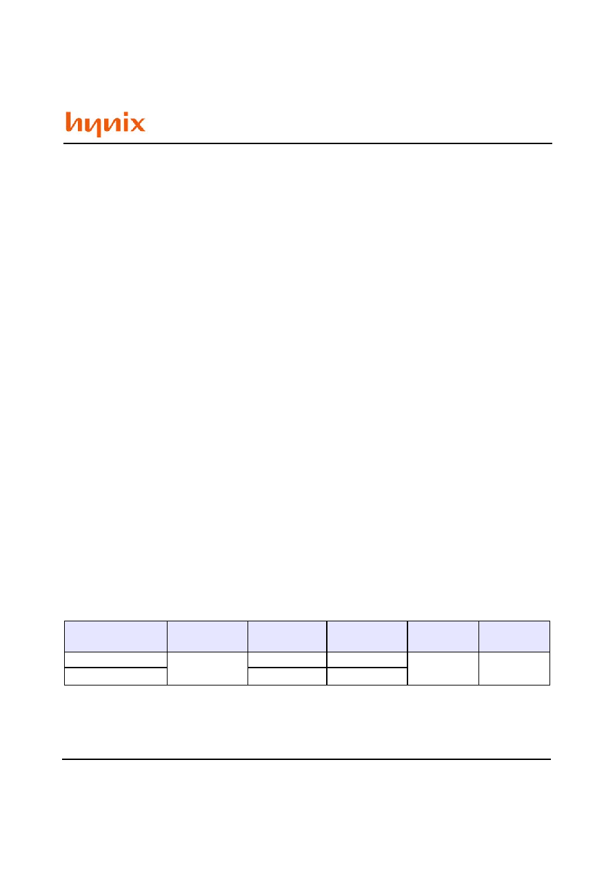
ORDERING INFORMATION
Part No.
Power Supply
Clock
Frequency
Max Data Rate
interface
Package
HY5DU561622DT-5
VDD=2.5V
VDDQ=2.5V
200MHz
400Mbps/pin
SSTL-2
400mil 66pin
TSOP-II
HY5DU561622DT-6
166MHz
333Mbps/pin
相關(guān)PDF資料 |
PDF描述 |
|---|---|
| HY5DU561622FTP-4I | 16M X 16 DDR DRAM, 0.7 ns, PDSO66 |
| HY5DU56422ALF-J | 64M X 4 DDR DRAM, 0.7 ns, PBGA60 |
| HY5MS5B6LF-H | 16M X 16 DDR DRAM, 6.5 ns, PBGA60 |
| HY5PS1G831ALFP-C4 | 128M X 8 DDR DRAM, PBGA68 |
| HY5PS1G831ALFP-Y5 | 128M X 8 DDR DRAM, PBGA68 |
相關(guān)代理商/技術(shù)參數(shù) |
參數(shù)描述 |
|---|---|
| HY5DU561622DTP | 制造商:HYNIX 制造商全稱:Hynix Semiconductor 功能描述:256M DDR SDRAM (268,435,456-bit CMOS Double Data Rate(DDR) Synchronous DRAM) |
| HY5DU561622DTP-H | 制造商:HYNIX 制造商全稱:Hynix Semiconductor 功能描述:256M DDR SDRAM (268,435,456-bit CMOS Double Data Rate(DDR) Synchronous DRAM) |
| HY5DU561622DTP-J | 制造商:SK Hynix Inc 功能描述:SDRAM, DDR, 16M x 16, 66 Pin, Plastic, TSSOP |
| HY5DU561622DTP-K | 制造商:HYNIX 制造商全稱:Hynix Semiconductor 功能描述:256M DDR SDRAM (268,435,456-bit CMOS Double Data Rate(DDR) Synchronous DRAM) |
| HY5DU561622DTP-L | 制造商:HYNIX 制造商全稱:Hynix Semiconductor 功能描述:256M DDR SDRAM (268,435,456-bit CMOS Double Data Rate(DDR) Synchronous DRAM) |
發(fā)布緊急采購(gòu),3分鐘左右您將得到回復(fù)。