- 您現(xiàn)在的位置:買賣IC網(wǎng) > PDF目錄385396 > HSP50214VI (INTERSIL CORP) Programmable Downconverter PDF資料下載
參數(shù)資料
| 型號(hào): | HSP50214VI |
| 廠商: | INTERSIL CORP |
| 元件分類: | 通信及網(wǎng)絡(luò) |
| 英文描述: | Programmable Downconverter |
| 中文描述: | SPECIALTY TELECOM CIRCUIT, PQFP120 |
| 封裝: | MQFP-120 |
| 文件頁數(shù): | 33/54頁 |
| 文件大?。?/td> | 395K |
| 代理商: | HSP50214VI |
第1頁第2頁第3頁第4頁第5頁第6頁第7頁第8頁第9頁第10頁第11頁第12頁第13頁第14頁第15頁第16頁第17頁第18頁第19頁第20頁第21頁第22頁第23頁第24頁第25頁第26頁第27頁第28頁第29頁第30頁第31頁第32頁當(dāng)前第33頁第34頁第35頁第36頁第37頁第38頁第39頁第40頁第41頁第42頁第43頁第44頁第45頁第46頁第47頁第48頁第49頁第50頁第51頁第52頁第53頁第54頁
33
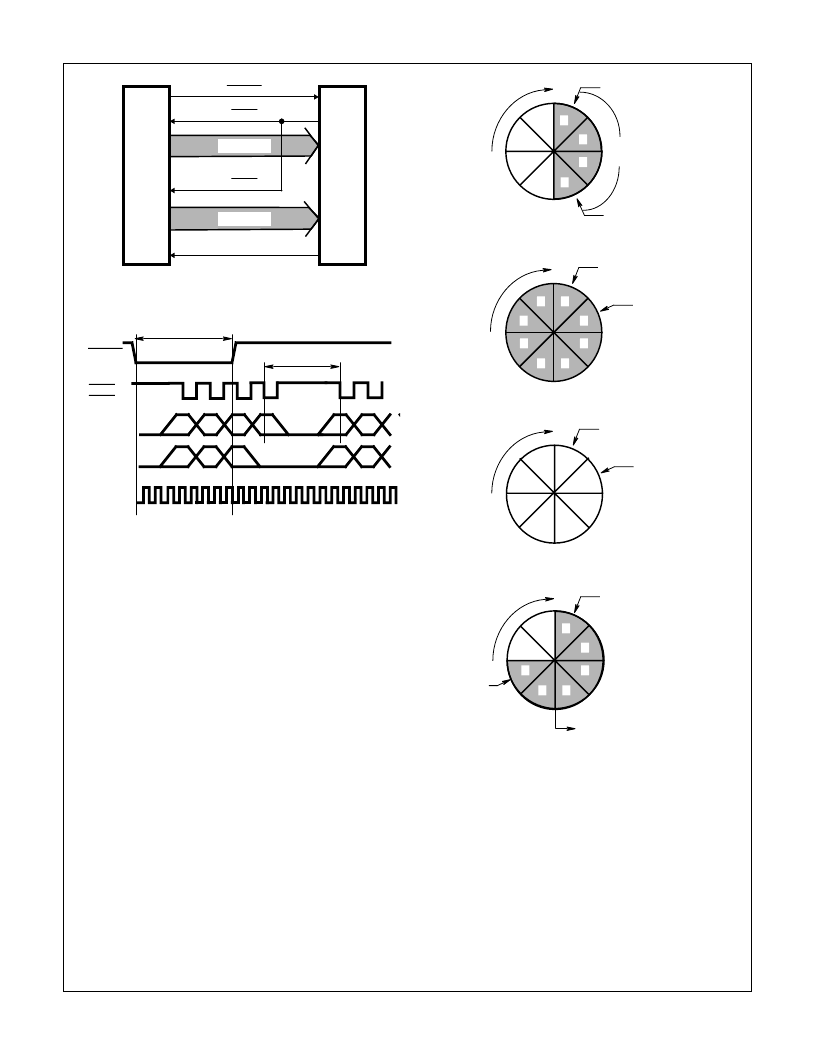
Suppose the depth of the Buffer RAM Output section is pro-
grammed for an INTRRP pointer depth of 4. If the output is at 4
times the baud rate, the processing routine for the microprocessor
may only need to read the buffer when the Buffer RAM had 4
samples since processing is usually on a baud by baud basis.
Figure 37 illustrates the conceptual view of the FIFO as a circular
buffer, with the Write address one step ahead of the read
address.
Figure 37A deals with clockwise read and write address incre-
menting. The FIFO depth is the difference between the Write and
Read pointers, modulo 8. Figure 37B illustrates a FIFO status of
Full, while Figure 37C illustrates a FIFO empty status condition.
Figure 37D illustrates a programmed FIFO depth of 3 and the
INTRRP signal indicating that the buffer has sufficient data to be
read.Following some simple rules for operating the FIFO will elim-
inate most operational errors:
Rule #1: The Read and Write Pointers cannot point at the same
address (the circuitry will not allow this).
Rule #2: The FIFO is full when the Write Address = Read
Address -1 (no more data will be written until some samples are
read or the FIFO is reset).
Rule #3: The FIFO is empty when the Read Address = (Write
Address -1) (the circuitry will not allow the read pointer to be
incremented).
Rule #4: You cannot write over what you have not read.
Rule #5: RESET places the Write address pointer = 000 and
Read address pointer = 111.
Rule #6: The best addressing scheme is to read the FIFO until it
is empty. This avoids erroneous INTRRP assertions and provides
for simple FIFO depth monitoring. The interrupt is generated
when the depth increments past the threshold
.
H
INTRRP
OEAL
OEBL
PDC
16-BIT
μ
P
SEL(2:0)
BOUT(7:0)
AOUT(7:0)
FIGURE 35. INTERFACE BETWEEN A 16-BIT MICROPROCES-
SOR AND PDC IN FIFO BUFFER RAM MODE
INT
RD
D(15:8)
D(7:0)
A(2:0)
1
2 3 4
1 2 3 4
5 6 7 8
0
1
4
7
0
1
INTRRP
OEAL,
OEBL
SEL(0:2)
I
Q
FR
I
Q
AOUT(7:0),
BOUT(7:0)
PROCCLK
8 CLKS
> 4 CLKS
FIGURE 36. TIMING DIAGRAM FOR PDC IN FIFO MODE WITH
OUTPUTS I, Q, AND FREQUENCY SENT TO
AOUT(7:0) AND BOUT(7:0)
FIGURE 37. FIFO REGISTER OPERATION
READ
WRITE
FIFO
DEPTH
WRITE
READ
READ
WRITE
WRITE
READ
READY
A: FIFO DEPTH IS (WRITE - READ)
B: FIFO FULL IS WHEN (WRITE - READ) = 7
C: FIFO EMPTY IS WHEN (WRITE - READ) = 1
D: FIFO READY IS WHEN (WRITE - READ) > DEPTH
1
2
3
4
5
6
7
0
1
2
3
4
5
6
7
0
1
2
3
4
5
6
7
0
1
2
3
4
5
6
7
0
HSP50214
相關(guān)PDF資料 |
PDF描述 |
|---|---|
| HSP50214 | Programmable Downconverter |
| HSP50215VC | Digital UpConverter |
| HSP50215VI | Digital UpConverter |
| HSP50215EVAL | DSP Modulator Evaluation Board |
| HSP50215 | Digital UpConverter(數(shù)字上變頻器) |
相關(guān)代理商/技術(shù)參數(shù) |
參數(shù)描述 |
|---|---|
| HSP50215 | 制造商:INTERSIL 制造商全稱:Intersil Corporation 功能描述:DSP Modulator Evaluation Board |
| HSP50215EVAL | 制造商:INTERSIL 制造商全稱:Intersil Corporation 功能描述:DSP Modulator Evaluation Board |
| HSP50215VC | 制造商:INTERSIL 制造商全稱:Intersil Corporation 功能描述:Digital UpConverter |
| HSP50215VI | 制造商:INTERSIL 制造商全稱:Intersil Corporation 功能描述:Digital UpConverter |
| HSP50216 | 制造商:INTERSIL 制造商全稱:Intersil Corporation 功能描述:Four-Channel Programmable Digital Downconverter |
發(fā)布緊急采購,3分鐘左右您將得到回復(fù)。