- 您現(xiàn)在的位置:買賣IC網(wǎng) > PDF目錄385354 > HC4046 (System Logic Semiconductor Co., Ltd.) Phase-Locked Loop PDF資料下載
參數(shù)資料
| 型號: | HC4046 |
| 廠商: | System Logic Semiconductor Co., Ltd. |
| 英文描述: | Phase-Locked Loop |
| 中文描述: | 鎖相環(huán) |
| 文件頁數(shù): | 1/12頁 |
| 文件大?。?/td> | 134K |
| 代理商: | HC4046 |

SL74HC4046
S ystem Logic
Semiconductor
SLS
Phase-Locked Loop
High-Performance Silicon-Gate CMOS
The device inputs are compatible with standard CMOS outputs;
with pullup resistors, they are compatible with LS/ALSTTL outputs.
The SL74HC4046 phase-locked loop contains three phase
comparators, a voltage-controlled oscillator (VCO) and unity gain op-
amp DEM
OUT
. The comparators have two common signal inputs,
COMP
IN
, and SIG
IN
. Input SIG
IN
and COMP
IN
can be used directly
coupled to large voltage signals, or indirectly coupled (with a series
capacitor to small voltage signals). The self-bias circuit adjusts small
voltage signals in the linear region of the amplifier. Phase comparator 1
(an exclusive OR gate) provides a digital error signal PC1
OUT
and
maintains 90 degrees phase shift at the center frequency between SIG
IN
and COMP
IN
signals (both at 50% duty cycle). Phase comparator 2
(with leading-edge sensing logic) provides digital error signals PC2
OUT
and PCP
OUT
and maintains a 0 degree phase shift between SIG
IN
and
COMP
IN
signals (duty cycle is immaterial). The linear VCO produces an
output signal VCO
OUT
whose frequency is determined by the voltage of
input VCO
IN
signal and the capacitor and resistors connected to pins
C1A, C1B, R1 and R2. The unity gain op-amp output DEM
OUT
with an external resistor is used where the VCO
IN
signal is needed but no loading can be tolerated. The inhibit input, when high, disables the VCO and all on-amps
to minimize standby power consumption.
Applications include FM and FSK modulation and demodulation, frequency synthesis and multiplication,
frequency discrimination, tone decoding, data synchronization and conditioning, voltage-to-frequency
conversion and motor speed control.
Low Power Consumption Characteristic of CMOS Device
Operating Speeds Similary to LS/ALSTTL
Wide Operating Voltage Range: 3.0 to 6.0 V
Low Input Current: 1.0
μ
A Maximum (except SIG
IN
and
COMP
IN
)
Low Quiescent Current: 80
μ
A Maximum (VCO disabled)
High Noise Immunity Characteristic of CMOS Devices
Diode Protection on all Inputs
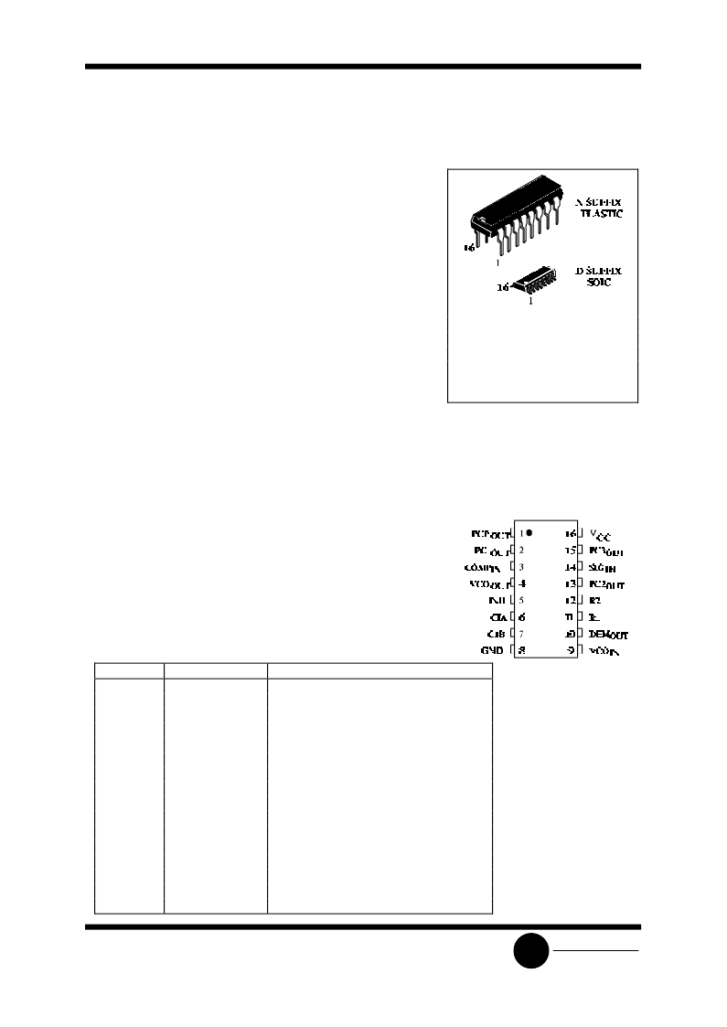
Pin No.
1
2
3
4
5
6
7
8
9
10
11
12
13
14
15
16
Symbol
PCP
OUT
PC1
OUT
COMP
IN
VCO
OUT
INH
C1A
C1B
GND
VCO
IN
DEM
OUT
R1
R2
PC2
OUT
SIG
IN
PC3
OUT
V
CC
Name and Function
Phase Comparator Pulse Output
Phase Comparator 1 Output
Comparator Input
VCO Output
Inhibit Input
Capacitor C1 Connection A
Capacitor C1 Connection B
Ground (0 V) V
SS
VCO Input
Demodulator Output
Resistor R1 Connection
Resistor R2 Connection
Phase Comparator 2 Output
Signal Input
Phase Comparator 3 Output
Positive Supply Voltage
ORDERING INFORMATION
SL74HC4046N Plastic
SL74HC4046D SOIC
T
A
= -55
°
to 125
°
C for all packages
PIN ASSIGNMENT
相關(guān)PDF資料 |
PDF描述 |
|---|---|
| HC4053 | IC-VLTG REG 125V-1A |
| HC4094 | T-NPN-SI HIGH VLTG AMP |
| HC49J | SM Crystal Formed Leads |
| HC534 | Voltage Regulator IC; Package/Case:3-TO-3; Current Rating:1.5A; Output Voltage Max:-12V; Voltage Regulator Type:Fixed Voltage; Mounting Type:Through Hole |
| HC5503CBZ | Low Cost 24V SLIC For PABX / Key Systems |
相關(guān)代理商/技術(shù)參數(shù) |
參數(shù)描述 |
|---|---|
| HC4046A | 制造商:Motorola Inc 功能描述: |
| HC-405 | 制造商:Thomas & Betts 功能描述: |
| HC4051A-L85H WAF | 制造商:ON Semiconductor 功能描述: |
| HC4052 | 制造商:SLS 制造商全稱:System Logic Semiconductor 功能描述:Analog Multiplexer/Demultiplexer(High-Performance Silicon-Gate CMOS) |
| HC4052A-L85H WAF | 制造商:ON Semiconductor 功能描述: |
發(fā)布緊急采購,3分鐘左右您將得到回復(fù)。