- 您現(xiàn)在的位置:買(mǎi)賣(mài)IC網(wǎng) > PDF目錄375853 > FM8P51EF (Electronic Theatre Controls, Inc.) EPROM/ROM-Based 8-Bit Microcontroller PDF資料下載
參數(shù)資料
| 型號(hào): | FM8P51EF |
| 廠商: | Electronic Theatre Controls, Inc. |
| 英文描述: | EPROM/ROM-Based 8-Bit Microcontroller |
| 中文描述: | 存儲(chǔ)器/基于ROM的8位微控制器 |
| 文件頁(yè)數(shù): | 19/60頁(yè) |
| 文件大?。?/td> | 369K |
| 代理商: | FM8P51EF |
第1頁(yè)第2頁(yè)第3頁(yè)第4頁(yè)第5頁(yè)第6頁(yè)第7頁(yè)第8頁(yè)第9頁(yè)第10頁(yè)第11頁(yè)第12頁(yè)第13頁(yè)第14頁(yè)第15頁(yè)第16頁(yè)第17頁(yè)第18頁(yè)當(dāng)前第19頁(yè)第20頁(yè)第21頁(yè)第22頁(yè)第23頁(yè)第24頁(yè)第25頁(yè)第26頁(yè)第27頁(yè)第28頁(yè)第29頁(yè)第30頁(yè)第31頁(yè)第32頁(yè)第33頁(yè)第34頁(yè)第35頁(yè)第36頁(yè)第37頁(yè)第38頁(yè)第39頁(yè)第40頁(yè)第41頁(yè)第42頁(yè)第43頁(yè)第44頁(yè)第45頁(yè)第46頁(yè)第47頁(yè)第48頁(yè)第49頁(yè)第50頁(yè)第51頁(yè)第52頁(yè)第53頁(yè)第54頁(yè)第55頁(yè)第56頁(yè)第57頁(yè)第58頁(yè)第59頁(yè)第60頁(yè)

FM8P51
Rev1.2 Mar 15, 2005
P.19/FM8P51
FEELING
TECHNOLOGY
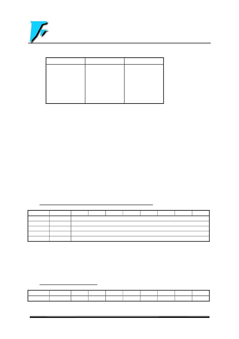
PS2:PS0
: Prescaler rate select bits.
PS2:PS0
Timer0 Rate
WDT Rate
0 0 0
0 0 1
0 1 0
0 1 1
1 0 0
1 0 1
1 1 0
1 1 1
1:2
1:4
1:8
1:16
1:32
1:64
1:128
1:256
1:1
1:2
1:4
1:8
1:16
1:32
1:64
1:128
PSA
: Prescaler assign bit.
= 1, WDT (watch-dog timer).
= 0, TMR0 (Timer0).
GIE
: Global interrupt enable bit.
= 0, Disable all interrupts. For wake-up from SLEEP mode through an interrupt event, the device will continue
execution at the instruction after the SLEEP instruction.
= 1, Enable all un-masked interrupts. For wake-up from SLEEP mode through an interrupt event, the device
will branch to the interrupt address (001h).
Note : 1. The GIE bit is not writable bit. This bit is only set by ENI or RETFIE instructions, and cleared by DISI
instruction or entering into interrupt subroutine.
2. When an interrupt event occur with the GIE bit and its corresponding interrupt enable bit are all set,
the GIE bit will be cleared by hardware to disable any further interrupts. The RETFIE instruction will
exit the interrupt routine and set the GIE bit to re-enable interrupt.
/PHBCE
: = 0, Enable the internal pull-high of IOB0~ IOB7, IOC4~IOC5, and IOE0~IOE5 pins.
= 1, Disable the internal pull-high of IOB0~ IOB7, IOC4~IOC5, and IOE0~IOE5 pins.
Note : /PHB, /PHE are “AND” gating with /PHBCE, that is each one written “0” will enable pull-high.
2.1.32 IOSTA, IOSTB, IOSTC, IOSTD & IOSTE (Port I/O Control Registers)
Address
Name
B7
B6
B5
05h (r/w)
IOSTA
Port A I/O Control Register
06h (r/w)
IOSTB
Port B I/O Control Register
07h (r/w)
IOSTC
Port C I/O Control Register
08h (r/w)
IOSTD
Port D I/O Control Register
09h (r/w)
IOSTE
Port E I/O Control Register
Accessed by IOST/IOSTR instructions.
The Port I/O Control Registers are loaded with the contents of the ACC Register by executing the IOST R (05h~09h)
instruction. By executing the IOSTR instruction, user can read these registers into ACC.
A ‘1’ from a IOST Register bit puts the corresponding output driver in hi-impedance state (input mode). A ‘0’ enables
the output buffer and puts the contents of the output data latch on the selected pins (output mode).
The IOST Registers are set all “1”s (output drivers disabled) upon RESET.
2.1.33 T1CON (Timer 1 Control Register)
Address
Name
B7
B6
B5
0Ch (r/w)
T1CON
Accessed by IOST/IOSTR instructions.
B4
B3
B2
B1
B0
B4
B3
B2
T1ON
B1
T1P1
B0
T1P0
相關(guān)PDF資料 |
PDF描述 |
|---|---|
| FM8P51EP | EPROM/ROM-Based 8-Bit Microcontroller |
| FM8P51F | EPROM/ROM-Based 8-Bit Microcontroller |
| FM8P51P | EPROM/ROM-Based 8-Bit Microcontroller |
| FM8P51E | EPROM/ROM-Based 8-Bit Microcontroller |
| FM8P54 | EPROM/ROM-Based 8-Bit Microcontroller Series |
相關(guān)代理商/技術(shù)參數(shù) |
參數(shù)描述 |
|---|---|
| FM8P51EP | 制造商:未知廠家 制造商全稱(chēng):未知廠家 功能描述:EPROM/ROM-Based 8-Bit Microcontroller |
| FM8P51F | 制造商:未知廠家 制造商全稱(chēng):未知廠家 功能描述:EPROM/ROM-Based 8-Bit Microcontroller |
| FM8P51P | 制造商:未知廠家 制造商全稱(chēng):未知廠家 功能描述:EPROM/ROM-Based 8-Bit Microcontroller |
| FM8P54 | 制造商:未知廠家 制造商全稱(chēng):未知廠家 功能描述:EPROM/ROM-Based 8-Bit Microcontroller Series |
| FM8P54E | 制造商:未知廠家 制造商全稱(chēng):未知廠家 功能描述:EPROM/ROM-Based 8-Bit Microcontroller Series |
發(fā)布緊急采購(gòu),3分鐘左右您將得到回復(fù)。