- 您現(xiàn)在的位置:買賣IC網(wǎng) > PDF目錄4344 > EP4SGX70HF35I4N (Altera)IC STRATIX IV FPGA 70K 1152FBGA PDF資料下載
參數(shù)資料
| 型號(hào): | EP4SGX70HF35I4N |
| 廠商: | Altera |
| 文件頁(yè)數(shù): | 72/82頁(yè) |
| 文件大小: | 0K |
| 描述: | IC STRATIX IV FPGA 70K 1152FBGA |
| 產(chǎn)品培訓(xùn)模塊: | Three Reasons to Use FPGA's in Industrial Designs |
| 標(biāo)準(zhǔn)包裝: | 3 |
| 系列: | Stratix® IV GX |
| LAB/CLB數(shù): | 2904 |
| 邏輯元件/單元數(shù): | 72600 |
| RAM 位總計(jì): | 7564880 |
| 輸入/輸出數(shù): | 488 |
| 電源電壓: | 0.87 V ~ 0.93 V |
| 安裝類型: | 表面貼裝 |
| 工作溫度: | -40°C ~ 100°C |
| 封裝/外殼: | 1152-BBGA |
| 供應(yīng)商設(shè)備封裝: | 1152-FBGA(27x27) |
第1頁(yè)第2頁(yè)第3頁(yè)第4頁(yè)第5頁(yè)第6頁(yè)第7頁(yè)第8頁(yè)第9頁(yè)第10頁(yè)第11頁(yè)第12頁(yè)第13頁(yè)第14頁(yè)第15頁(yè)第16頁(yè)第17頁(yè)第18頁(yè)第19頁(yè)第20頁(yè)第21頁(yè)第22頁(yè)第23頁(yè)第24頁(yè)第25頁(yè)第26頁(yè)第27頁(yè)第28頁(yè)第29頁(yè)第30頁(yè)第31頁(yè)第32頁(yè)第33頁(yè)第34頁(yè)第35頁(yè)第36頁(yè)第37頁(yè)第38頁(yè)第39頁(yè)第40頁(yè)第41頁(yè)第42頁(yè)第43頁(yè)第44頁(yè)第45頁(yè)第46頁(yè)第47頁(yè)第48頁(yè)第49頁(yè)第50頁(yè)第51頁(yè)第52頁(yè)第53頁(yè)第54頁(yè)第55頁(yè)第56頁(yè)第57頁(yè)第58頁(yè)第59頁(yè)第60頁(yè)第61頁(yè)第62頁(yè)第63頁(yè)第64頁(yè)第65頁(yè)第66頁(yè)第67頁(yè)第68頁(yè)第69頁(yè)第70頁(yè)第71頁(yè)當(dāng)前第72頁(yè)第73頁(yè)第74頁(yè)第75頁(yè)第76頁(yè)第77頁(yè)第78頁(yè)第79頁(yè)第80頁(yè)第81頁(yè)第82頁(yè)
1–66
Chapter 1: DC and Switching Characteristics for Stratix IV Devices
Glossary
Stratix IV Device Handbook
March 2014
Altera Corporation
Volume 4: Device Datasheet and Addendum
S
SW (sampling
window)
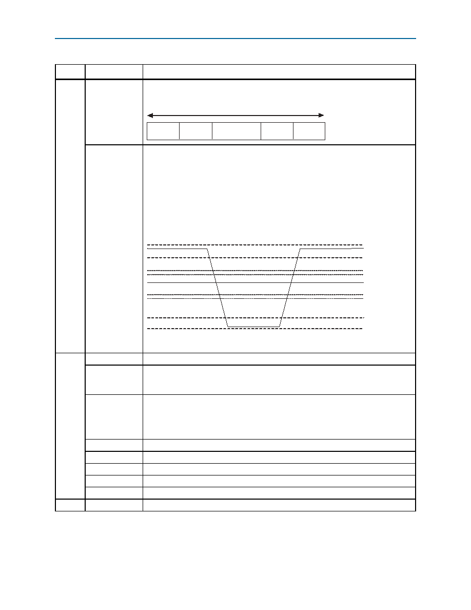
Timing Diagram—the period of time during which the data must be valid in order to capture
it correctly. The setup and hold times determine the ideal strobe position within the sampling
window, as shown:
Single-ended
voltage
referenced I/O
standard
The JEDEC standard for SSTl and HSTL I/O defines both the AC and DC input signal values.
The AC values indicate the voltage levels at which the receiver must meet its timing
specifications. The DC values indicate the voltage levels at which the final logic state of the
receiver is unambiguously defined. After the receiver input has crossed the AC value, the
receiver changes to the new logic state.
The new logic state is then maintained as long as the input stays beyond the AC threshold.
This approach is intended to provide predictable receiver timing in the presence of input
waveform ringing, as shown:
Single-Ended Voltage Referenced I/O Standard
T
tC
High-speed receiver/transmitter input and output clock period.
TCCS (channel-
to-channel-skew)
The timing difference between the fastest and slowest output edges, including tCO variation
and clock skew, across channels driven by the same PLL. The clock is included in the TCCS
measurement (refer to the Timing Diagram figure under SW in this table).
tDUTY
High-speed I/O block: Duty cycle on high-speed transmitter output clock.
Timing Unit Interval (TUI)
The timing budget allowed for skew, propagation delays, and data sampling window.
(TUI = 1/(Receiver Input Clock Frequency Multiplication Factor) = tC/w)
tFALL
Signal high-to-low transition time (80-20%)
tINCCJ
Cycle-to-cycle jitter tolerance on the PLL clock input
tOUTPJ_IO
Period jitter on the general purpose I/O driven by a PLL
tOUTPJ_DC
Period jitter on the dedicated clock output driven by a PLL
tRISE
Signal low-to-high transition time (20-80%)
U
——
Table 1–54. Glossary Table (Part 3 of 4)
Letter
Subject
Definitions
Bit Time
0.5 x TCCS
RSKM
Sampling Window
(SW)
RSKM
0.5 x TCCS
VIH(AC)
VIH(DC)
VREF
VIL(DC)
VIL(AC)
VOH
VOL
VCCIO
VSS
相關(guān)PDF資料 |
PDF描述 |
|---|---|
| EP2AGX125DF25I5 | IC ARRIA II GX FPGA 125K 572FBGA |
| 24LC01B/ST | IC EEPROM 1KBIT 400KHZ 8TSSOP |
| EP2AGX125DF25C4 | IC ARRIA II GX FPGA 125K 572FBGA |
| EP1SGX25FF1020C6 | IC STRATIX GX FPGA 25K 1020-FBGA |
| ABB92DHFD-S329 | EDGECARD PCI 184PS .050 SMD 3.3V |
相關(guān)代理商/技術(shù)參數(shù) |
參數(shù)描述 |
|---|---|
| EP4-SI | 制造商:Box Enclosures & Assembly Services 功能描述:END PLATE FOR SERIES 4, SILVER ANODIZED, 2.11 H X 6.68 W 制造商:Box Enclosures & Assembly Services 功能描述:Enclosure End Plate 制造商:Box Enclosures & Assembly Services 功能描述:END PLATE; Accessory Type:End Plate; For Use With:Extruded Aluminum Enclosures, BEX Series 4; Body Color:Silver; Body Material:Aluminum; External Height:2.11"; External Width:6.68"; Features:Silver; Leaded Process Compatible:Yes ;RoHS Compliant: Yes |
| EP4-SPR-BULK | 功能描述:SONIC DEFENDER SMALL CLEAR RoHS:是 類別:音頻產(chǎn)品 >> 配件 系列:EarPro 標(biāo)準(zhǔn)包裝:1 系列:- 附件類型:墊圈 材質(zhì):氯丁橡膠 顏色:黑 適用于相關(guān)產(chǎn)品:Sonalert? 信號(hào)設(shè)備 其它名稱:458-1048 |
| EP5 | 制造商:Datak Corporation 功能描述: |
| EP-5 | 制造商:Mac8 功能描述: 制造商:Curtis Industries 功能描述: |
| EP501 | 制造商:ACTEL 制造商全稱:Actel Corporation 功能描述:EP501 NAND Flash Controller |
發(fā)布緊急采購(gòu),3分鐘左右您將得到回復(fù)。