- 您現(xiàn)在的位置:買賣IC網(wǎng) > PDF目錄1916 > DS33R41+ (Maxim Integrated Products)IC TXRX ETHERNET MAP 400-BGA PDF資料下載
參數(shù)資料
| 型號: | DS33R41+ |
| 廠商: | Maxim Integrated Products |
| 文件頁數(shù): | 146/335頁 |
| 文件大?。?/td> | 0K |
| 描述: | IC TXRX ETHERNET MAP 400-BGA |
| 產(chǎn)品培訓(xùn)模塊: | Lead (SnPb) Finish for COTS Obsolescence Mitigation Program |
| 標(biāo)準(zhǔn)包裝: | 1 |
| 類型: | 收發(fā)器 |
| 驅(qū)動器/接收器數(shù): | 4/4 |
| 規(guī)程: | T1/E1/J1 |
| 電源電壓: | 3.14 V ~ 3.47 V |
| 安裝類型: | 表面貼裝 |
| 封裝/外殼: | 400-BBGA |
| 供應(yīng)商設(shè)備封裝: | 400-PBGA(27x27) |
| 包裝: | 托盤 |
| 產(chǎn)品目錄頁面: | 1429 (CN2011-ZH PDF) |
第1頁第2頁第3頁第4頁第5頁第6頁第7頁第8頁第9頁第10頁第11頁第12頁第13頁第14頁第15頁第16頁第17頁第18頁第19頁第20頁第21頁第22頁第23頁第24頁第25頁第26頁第27頁第28頁第29頁第30頁第31頁第32頁第33頁第34頁第35頁第36頁第37頁第38頁第39頁第40頁第41頁第42頁第43頁第44頁第45頁第46頁第47頁第48頁第49頁第50頁第51頁第52頁第53頁第54頁第55頁第56頁第57頁第58頁第59頁第60頁第61頁第62頁第63頁第64頁第65頁第66頁第67頁第68頁第69頁第70頁第71頁第72頁第73頁第74頁第75頁第76頁第77頁第78頁第79頁第80頁第81頁第82頁第83頁第84頁第85頁第86頁第87頁第88頁第89頁第90頁第91頁第92頁第93頁第94頁第95頁第96頁第97頁第98頁第99頁第100頁第101頁第102頁第103頁第104頁第105頁第106頁第107頁第108頁第109頁第110頁第111頁第112頁第113頁第114頁第115頁第116頁第117頁第118頁第119頁第120頁第121頁第122頁第123頁第124頁第125頁第126頁第127頁第128頁第129頁第130頁第131頁第132頁第133頁第134頁第135頁第136頁第137頁第138頁第139頁第140頁第141頁第142頁第143頁第144頁第145頁當(dāng)前第146頁第147頁第148頁第149頁第150頁第151頁第152頁第153頁第154頁第155頁第156頁第157頁第158頁第159頁第160頁第161頁第162頁第163頁第164頁第165頁第166頁第167頁第168頁第169頁第170頁第171頁第172頁第173頁第174頁第175頁第176頁第177頁第178頁第179頁第180頁第181頁第182頁第183頁第184頁第185頁第186頁第187頁第188頁第189頁第190頁第191頁第192頁第193頁第194頁第195頁第196頁第197頁第198頁第199頁第200頁第201頁第202頁第203頁第204頁第205頁第206頁第207頁第208頁第209頁第210頁第211頁第212頁第213頁第214頁第215頁第216頁第217頁第218頁第219頁第220頁第221頁第222頁第223頁第224頁第225頁第226頁第227頁第228頁第229頁第230頁第231頁第232頁第233頁第234頁第235頁第236頁第237頁第238頁第239頁第240頁第241頁第242頁第243頁第244頁第245頁第246頁第247頁第248頁第249頁第250頁第251頁第252頁第253頁第254頁第255頁第256頁第257頁第258頁第259頁第260頁第261頁第262頁第263頁第264頁第265頁第266頁第267頁第268頁第269頁第270頁第271頁第272頁第273頁第274頁第275頁第276頁第277頁第278頁第279頁第280頁第281頁第282頁第283頁第284頁第285頁第286頁第287頁第288頁第289頁第290頁第291頁第292頁第293頁第294頁第295頁第296頁第297頁第298頁第299頁第300頁第301頁第302頁第303頁第304頁第305頁第306頁第307頁第308頁第309頁第310頁第311頁第312頁第313頁第314頁第315頁第316頁第317頁第318頁第319頁第320頁第321頁第322頁第323頁第324頁第325頁第326頁第327頁第328頁第329頁第330頁第331頁第332頁第333頁第334頁第335頁
DS33R41 Inverse-Multiplexing Ethernet Mapper with Quad Integrated T1/E1/J1 Transceivers
23 of 335
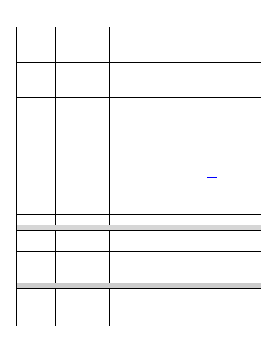
NAME
PIN
TYPE
FUNCTION
TXD[0]
TXD[1]
TXD[2]
TXD[3]
L20
M19
M18
M20
O
Transmit Data 0 through 3(MII).
TXD [3:0] is presented synchronously
with the rising edge of TX_CLK. TXD [0] is the least significant bit of the
data. When TX_EN is low the data on TXD should be ignored.
Transmit Data 0 through 1(RMII).
Two bits of data TXD [1:0] presented
synchronously with the rising edge of REF_CLK.
TX_EN
L19
O
Transmit Enable (MII).
This pin is asserted high when data TXD [3:0] is
being provided by the DS33R41. The signal is deasserted prior to the first
nibble of the next frame. This signal is synchronous with the rising edge
TX_CLK. It is asserted with the first bit of the preamble.
Transmit Enable (RMII).
When this signal is asserted, the data on TXD
[1:0] is valid. This signal is synchronous to the REF_CLK.
REF_CLK
C20
I
Reference Clock (RMII and MII).
When in RMII mode, all signals from
the PHY are synchronous to this clock input for both transmit and receive.
This required clock can be up to 50MHz and should have
±100ppm
accuracy.
When in MII mode in DCE operation, the DS33R41 uses this input to
generate the RX_CLK and TX_CLK outputs as required for the Ethernet
PHY interface. When the MII interface is used with DTE operation, this
clock is not required and should be tied low.
In DCE and RMII modes, this input must have a stable clock input before
setting the RST pin high for normal operation.
REF_CLKO
G19
O
Reference Clock Output (RMII and MII).
A derived clock output up to
50MHz, generated by internal division of the SYSCLKI signal. Frequency
accuracy of the REF_CLKO signal will be proportional to the accuracy of
the user-supplied SYSCLKI signal. See Section 9.1.2 for more
information.
DCEDTES
L17
I
DCE or DTE Selection.
The user must set this pin high for DCE Mode
selection or low for DTE Mode. In DCE Mode, the DS33R41 MAC port
can be directly connected to another MAC. In DCE Mode, the Transmit
clock (TX_CLK) and Receive clock (RX_CLK) are output by the
DS33R41. Note that there is no software bit selection of DCEDTES. Note
that DCE Mode is only relevant when the MAC interface is in MII mode.
RMIIMIIS
K13
I
RMII or MII Selection.
Set high to configure the MAC for RMII interfacing.
Set low for MII interfacing.
PHY MANAGEMENT BUS
MDC
E20
O
Management Data Clock (MII).
Clocks management data between the
PHY and DS33R41. The clock is derived from the SYSCLKI, with a
maximum frequency is 1.67MHz. The user must leave this pin
unconnected in the DCE Mode.
MDIO
F20
IO
MII Management data IO (MII).
Data path for control information between
the PHY and DS33R41. When not used, pull to logic high externally
through a 10k
Ω resistor. The MDC and MDIO pins are used to write or
read up to 32 Control and Status Registers in 32 PHY Controllers. This
port can also be used to initiate Auto-Negotiation for the PHY. The user
must leave this pin unconnected in the DCE Mode.
SDRAM CONTROLLER
SCAS
R14
O
SDRAM Column Address Strobe.
Active low output, used to latch the
column address on the rising edge of SDCLKO. It is used with commands
for Bank Activate, Precharge, and Mode Register Write.
SRAS
P15
O
SDRAM Row Address Strobe.
Active low output, used to latch the row
address on rising edge of SDCLKO. It is used with commands for Bank
Activate, Precharge, and Mode Register Write.
SDCS
R15
O
SDRAM Chip Select.
Active low output enables SDRAM access.
相關(guān)PDF資料 |
PDF描述 |
|---|---|
| DS33W11DK+ | IC MAPPING ETHERNET 256-CSBGA |
| DS33Z11+UNUSED | IC ETHERNET MAPPER 169-CSBGA |
| DS33Z44+ | IC MAPPER ETHERNET 256CSBGA |
| DS33ZH11+ | IC MAPPER ETHERNET 100CSBGA |
| DS34C87TN/NOPB | IC LINE DRIVER QUAD CMOS 16-DIP |
相關(guān)代理商/技術(shù)參數(shù) |
參數(shù)描述 |
|---|---|
| DS33R41+ | 功能描述:網(wǎng)絡(luò)控制器與處理器 IC Inv-Mult Enet Mapper w/Quad T1/E1/J1 Trx RoHS:否 制造商:Micrel 產(chǎn)品:Controller Area Network (CAN) 收發(fā)器數(shù)量: 數(shù)據(jù)速率: 電源電流(最大值):595 mA 最大工作溫度:+ 85 C 安裝風(fēng)格:SMD/SMT 封裝 / 箱體:PBGA-400 封裝:Tray |
| DS33W11+ | 功能描述:網(wǎng)絡(luò)控制器與處理器 IC Ethernet Over PDH Mapping Devices RoHS:否 制造商:Micrel 產(chǎn)品:Controller Area Network (CAN) 收發(fā)器數(shù)量: 數(shù)據(jù)速率: 電源電流(最大值):595 mA 最大工作溫度:+ 85 C 安裝風(fēng)格:SMD/SMT 封裝 / 箱體:PBGA-400 封裝:Tray |
| DS33W11DK+ | 功能描述:以太網(wǎng)開發(fā)工具 1/1 E-Net - PDH Design Kit RoHS:否 制造商:Micrel 產(chǎn)品:Evaluation Boards 類型:Ethernet Transceivers 工具用于評估:KSZ8873RLL 接口類型:RMII 工作電源電壓: |
| DS33W41+ | 功能描述:網(wǎng)絡(luò)控制器與處理器 IC Ethernet Over PDH Mapping Devices RoHS:否 制造商:Micrel 產(chǎn)品:Controller Area Network (CAN) 收發(fā)器數(shù)量: 數(shù)據(jù)速率: 電源電流(最大值):595 mA 最大工作溫度:+ 85 C 安裝風(fēng)格:SMD/SMT 封裝 / 箱體:PBGA-400 封裝:Tray |
| DS33X11+ | 功能描述:網(wǎng)絡(luò)控制器與處理器 IC Ethernet Over PDH Mapping Devices RoHS:否 制造商:Micrel 產(chǎn)品:Controller Area Network (CAN) 收發(fā)器數(shù)量: 數(shù)據(jù)速率: 電源電流(最大值):595 mA 最大工作溫度:+ 85 C 安裝風(fēng)格:SMD/SMT 封裝 / 箱體:PBGA-400 封裝:Tray |
發(fā)布緊急采購,3分鐘左右您將得到回復(fù)。