- 您現(xiàn)在的位置:買賣IC網(wǎng) > PDF目錄374016 > ADMCF341-EVALKIT (Analog Devices, Inc.) DashDSP⑩ 28-Lead Flash Mixed-Signal DSP with Enhanced Analog Front End PDF資料下載
參數(shù)資料
| 型號: | ADMCF341-EVALKIT |
| 廠商: | Analog Devices, Inc. |
| 英文描述: | DashDSP⑩ 28-Lead Flash Mixed-Signal DSP with Enhanced Analog Front End |
| 中文描述: | DashDSP⑩28引腳閃存混合信號增強(qiáng)的DSP與模擬前端 |
| 文件頁數(shù): | 16/36頁 |
| 文件大小: | 1106K |
| 代理商: | ADMCF341-EVALKIT |
第1頁第2頁第3頁第4頁第5頁第6頁第7頁第8頁第9頁第10頁第11頁第12頁第13頁第14頁第15頁當(dāng)前第16頁第17頁第18頁第19頁第20頁第21頁第22頁第23頁第24頁第25頁第26頁第27頁第28頁第29頁第30頁第31頁第32頁第33頁第34頁第35頁第36頁
REV. 0
–16–
ADMCF341
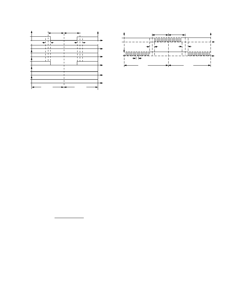
PWMCHA
= PWMCHB
PWMTM
PWMTM
AH
AL
BH
BL
2 PWMDT
2 PWMDT
CH
CL
Figure 9. An Example of PWM Signals Suitable for
ECM Control. PWMCHA = PWMCHB, BH/BL are a
Crossover Pair. AL, BH, CH, and CL Outputs are
Disabled. Operation Is in Single Update Mode.
Gate Drive Unit: PWMGATE Register
The gate drive unit of the PWM controller adds features that
simplify the design of isolated gate drive circuits for PWM
inverters. If a transformer-coupled power device gate drive
amplifier is used, the active PWM signal must be chopped at a
high frequency. The PWMGATE register allows the programming
of this high-frequency chopping mode. The chopped active
PWM signals may be required for the high side drivers only, for
the low side drivers only, or for both the high side and low side
switches. Therefore, independent control of this mode for both
high side and low side switches is included with two separate
control bits in the PWMGATE register.
Typical PWM output signals with high-frequency chopping
enabled on both high side and low side signals are shown in
Figure 10. Chopping of the high side PWM outputs (AH, BH
and CH) is enabled by setting Bit 8 of the PWMGATE register.
Chopping of the low side PWM outputs (AL, BL, and CL) is
enabled by setting Bit 9 of the PWMGATE register. The high
chopping frequency is controlled by the 8-bit word (GDCLK)
written to Bits 0 to 7 of the PWMGATE register. The period
and the frequency of this high-frequency carrier are:
¥
(
T
GDCLK
t
CHOP
CK
=
)
+
[
]
¥
4
1
f
f
GDCLK
(
CHOP
CLKOUT
=
¥
+
)
[
]
4
1
The GDCLK
value may range from 0 to 255, corresponding to
a programmable chopping frequency rate from 19.5 kHz to 5 MHz
for a 20 MHz CLKOUT rate. The gate drive features must
be programmed before operation of the PWM controller and
typically are not changed during normal operation of the PWM
controller. Following a reset, by default, all bits of the
PWMGATE register are cleared so that high-frequency chop-
ping is disabled.
PWMTM
PWMTM
[4
(GDCLK+1)]
2
PWMDT
2
PWMDT
PWMCHA
PWMCHA
AH
AL
Figure 10. Typical PWM Signals with High-
Frequency Gate Chopping Enabled on Both
High Side and Low Side Switches. (GDCLK Is
the Integer Equivalent of the Value in Bits 0
to 7 of the PWMGATE Register.)
PWM Shutdown
In the event of external fault conditions, it is essential that the
PWM system be instantaneously shut down. Two methods of
sensing a fault condition are provided by the ADMCF341. For
the first method, a low level on the
PWMTRIP
pin initiates an
instantaneous, asynchronous (independent of DSP clock) shut-
down of the PWM controller. This places all six PWM outputs
in the OFF state, disables the PWMSYNC pulse and associated
interrupt signal, and generates a
PWMTRIP
interrupt signal.
The
PWMTRIP
pin has an internal pull-down resistor so that
even if the pin becomes disconnected, the PWM outputs will be
disabled. The state of the
PWMTRIP
pin can be read from Bit 0
of the SYSSTAT register.
The second method for detecting a fault condition is through
the I
SENSE
pins of the analog block of the ADMCF341. When
the voltage at any of the I
SENSE
pins exceeds the trip threshold
(high or low), or the I
SENSE
pin is in high impedance (floating),
PWMTRIP
will be internally pulled low. The negative edge of
the internal
PWMTRIP
will generate a shutdown in the same
manner as a negative edge on pin
PWMTRIP
.
It is possible through software to initiate a PWM shutdown by
writing to the 1-bit read/write PWMSWT register (0x2061).
Writing to this bit generates a PWM shutdown in a manner
identical to the
PWMTRIP
or I
SENSE
pins. Following a PWM
shutdown, it is possible to determine if the shutdown was gener-
ated from hardware or software by reading the same PWMSWT
register. Reading this register also clears it.
Restarting the PWM after a fault condition is detected requires
clearing the fault and reinitializing the PWM. Clearing the fault
requires
PWMTRIP
to return to a HIGH state and I
SENSE
to
return to a voltage in the I
SENSE
trip level range. After the fault
has been cleared, the PWM can be restarted by writing to registers
PWMTM, PWMCHA, PWMCHB, and PWMCHC. After the
fault is cleared and the PWM registers are initialized, internal
timing of the three-phase timing unit will resume, and the new
duty cycle values will be latched on the next rising edge of
PWMSYNC.
PWM Registers
The configuration of the PWM registers is described at the end
of the data sheet. The parameters of the PWM block are tabu-
lated in Table V.
相關(guān)PDF資料 |
PDF描述 |
|---|---|
| ADN2811 | OC-48/OC-48 FEC Clock and Data Recovery IC with Integrated Limiting Amp |
| ADN2811ACP-CML | OC-48/OC-48 FEC Clock and Data Recovery IC with Integrated Limiting Amp |
| ADN2811ACP-CML-RL | OC-48/OC-48 FEC Clock and Data Recovery IC with Integrated Limiting Amp |
| ADN2812 | Continuous Rate 12.3 Mb/s to 2.7 Gb/s Clock and Data Recovery IC with Integrated Limiting Amp |
| ADN2812ACP | Continuous Rate 12.3 Mb/s to 2.7 Gb/s Clock and Data Recovery IC with Integrated Limiting Amp |
相關(guān)代理商/技術(shù)參數(shù) |
參數(shù)描述 |
|---|---|
| AD-MCX-RPSMAF | 功能描述:ADAPTER AU RPSMA FEM-MCX APPLE RoHS:是 類別:RF/IF 和 RFID >> RF配件 系列:* 標(biāo)準(zhǔn)包裝:1 系列:* |
| AD-MD3FF | 制造商:Pan Pacific 功能描述: |
| AD-MD4FF | 制造商:Pan Pacific 功能描述: |
| AD-MD6F/D5M | 制造商:Pan Pacific 功能描述: |
| AD-MD6FF | 制造商:Pan Pacific 功能描述: |
發(fā)布緊急采購,3分鐘左右您將得到回復(fù)。