- 您現(xiàn)在的位置:買賣IC網(wǎng) > PDF目錄374016 > ADM9240ARU (ANALOG DEVICES INC) Low Cost Microprocessor System Hardware Monitor PDF資料下載
參數(shù)資料
| 型號: | ADM9240ARU |
| 廠商: | ANALOG DEVICES INC |
| 元件分類: | 電源管理 |
| 英文描述: | Low Cost Microprocessor System Hardware Monitor |
| 中文描述: | 9-CHANNEL POWER SUPPLY SUPPORT CKT, PDSO24 |
| 封裝: | TSSOP-24 |
| 文件頁數(shù): | 18/22頁 |
| 文件大?。?/td> | 280K |
| 代理商: | ADM9240ARU |
ADM9240
–18–
REV. 0
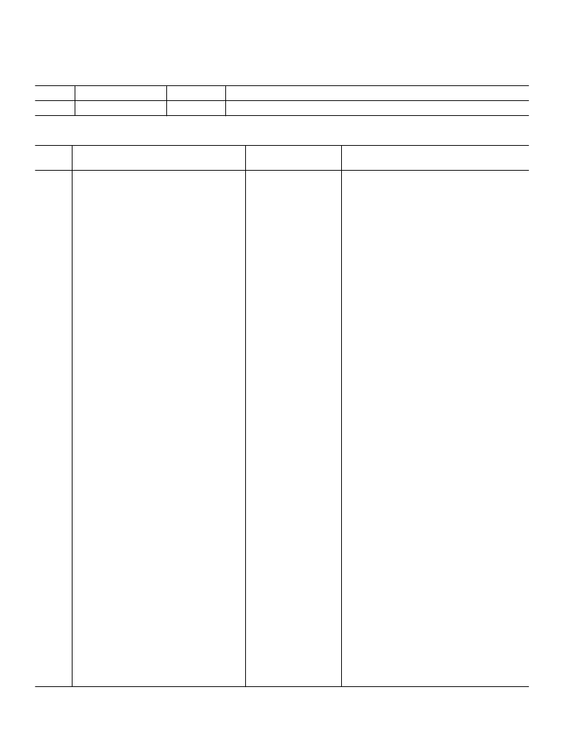
T able V. Address Pointer Register
Bit
Name
R/
W
Description
7–0
Address Pointer
Write
Address of ADM9240 Registers. See the tables below for detail.
T able VI. List of Registers
Notes
A7–A0 (Binary Bit 7–0)
Address
Description
Power on Value
15h
T est Register
0000 0000
Setting Bit 0 of this register to 1 selects
shutdown mode.
Caution
: Do Not write to
any other bits in this register.
19h
20h
21h
22h
23h
24h
25h
26h
27h
28h
29h
2Ah
2Bh
2Ch
2Dh
2Eh
2Fh
30h
31h
32h
33h
34h
35h
36h
37h
38h
39h
3Ah
3Bh
3Ch
3Dh
3Eh
Programmed Value of Analog Output
+2.5 V Measured Value
+V
CCP1
Measured Value
+3.3 V Measured Value
+5 V Measured Value
+12 V Measured Value
V
CCP2
Measured Value
Reserved
T emperature Reading
FAN1 Reading
FAN2 Reading
Reserved
+2.5 V High Limit
+2.5 V Low Limit
+V
CCP1
High Limit
+V
CCP1
Low Limit
+3.3 V High Limit
+3.3 V Low Limit
+5 V High Limit
+5 V Low Limit
+12 V High Limit
+12V Low Limit
V
CCP2
High Limit
V
CCP2
Low Limit
Reserved
Reserved
Hot T emperature Limit (High)
Hot T emperature Hysteresis Limit (Low)
FAN1 Fan Count Limit
FAN2 Fan Count Limit
Reserved
Company ID Number
1111 1111
Indeterminate
Indeterminate
Indeterminate
Indeterminate
Indeterminate
Indeterminate
Indeterminate
Indeterminate
Indeterminate
Indeterminate
Indeterminate
Indeterminate
Indeterminate
Indeterminate
Indeterminate
Indeterminate
Indeterminate
Indeterminate
Indeterminate
Indeterminate
Indeterminate
Indeterminate
Indeterminate
Indeterminate
Indeterminate
Indeterminate
Indeterminate
Indeterminate
Indeterminate
Indeterminate
0010 0011
Read Only
Read Only
Read Only
Read Only
Read Only
Read Only
Read Only
Read Only
Read Only
T his location will contain the company
identification number (Read Only).
T his location will contain the revision
number of the part. (Read Only).
See T able VII
See T able VIII
See T able IX
See T able X
See T able X I
See T able X II
See T able X III
See T able X IV
See T able X V
See T able X VI
See T able X VII
3Fh
Revision Number
Die Revision
40h
41h
42h
43h
44h
45h
46h
47h
48h
49h
4Bh
Configuration Register
Interrupt
INT
Status Register 1
Interrupt
INT
Status Register 2
INT
Mask Register 1
INT
Mask Register 2
Compatibility Register
Chassis Intrusion Clear Register
VID0–3/Fan Divisor Register
Serial Address Register
VID4 Register
T emperature Configuration Register
0000 1000
0000 0000
0000 0000
0000 0000
0000 0000
0000 0000
0000 0000
0101 (VID3–VID0)
0010 11(A1)(A0)
1000 000(VID4)
0000 0001
相關(guān)PDF資料 |
PDF描述 |
|---|---|
| ADM9261 | Triple- Power Supply Monitor(3路電源監(jiān)視器) |
| ADM9264ARN-REEL | Quad Power Supply Monitor for Desktop PCs |
| ADM9264ARN-REEL7 | Quad Power Supply Monitor for Desktop PCs |
| ADM9264 | Quad Power Supply Monitor for Desktop PCs |
| ADM9264ARN | Quad Power Supply Monitor for Desktop PCs |
相關(guān)代理商/技術(shù)參數(shù) |
參數(shù)描述 |
|---|---|
| ADM9240ARU-REEL | 制造商:AD 制造商全稱:Analog Devices 功能描述:Low Cost Microprocessor System Hardware Monitor |
| ADM9240ARU-REEL7 | 制造商:Analog Devices 功能描述: |
| ADM9264 | 制造商:AD 制造商全稱:Analog Devices 功能描述:Quad Power Supply Monitor for Desktop PCs |
| ADM9264ARN | 制造商:Analog Devices 功能描述:Volt Supervisor Monitor 2.8V/3.3V/5V/12V 16-Pin SOIC N 制造商:Rochester Electronics LLC 功能描述:MULTI-SUPPLY HARDWARE MON - Bulk |
| ADM9264ARN-REEL | 制造商:Rochester Electronics LLC 功能描述:- Tape and Reel |
發(fā)布緊急采購,3分鐘左右您將得到回復(fù)。