- 您現(xiàn)在的位置:買賣IC網(wǎng) > PDF目錄165348 > ADE7757AARZ (ANALOG DEVICES INC) SPECIALTY ANALOG CIRCUIT, PDSO16 PDF資料下載
參數(shù)資料
| 型號(hào): | ADE7757AARZ |
| 廠商: | ANALOG DEVICES INC |
| 元件分類: | 模擬信號(hào)調(diào)理 |
| 英文描述: | SPECIALTY ANALOG CIRCUIT, PDSO16 |
| 封裝: | LEAD FREE, MS-012AC, SOIC-16 |
| 文件頁(yè)數(shù): | 5/24頁(yè) |
| 文件大?。?/td> | 391K |
| 代理商: | ADE7757AARZ |
第1頁(yè)第2頁(yè)第3頁(yè)第4頁(yè)當(dāng)前第5頁(yè)第6頁(yè)第7頁(yè)第8頁(yè)第9頁(yè)第10頁(yè)第11頁(yè)第12頁(yè)第13頁(yè)第14頁(yè)第15頁(yè)第16頁(yè)第17頁(yè)第18頁(yè)第19頁(yè)第20頁(yè)第21頁(yè)第22頁(yè)第23頁(yè)第24頁(yè)
Preliminary Technical Data
ADE7757A
Rev. PrE | Page 13 of 24
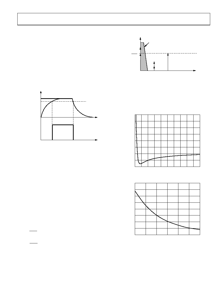
POWER SUPPLY MONITOR
The ADE7757A contains an on-chip power supply monitor.
The power supply (VDD) is continuously monitored by the
ADE7757A. If the supply is less than 4 V, the ADE7757A
becomes inactive. This is useful to ensure proper device
operation at power-up and power-down. The power supply
monitor has built in hysteresis and filtering that provide a high
degree of immunity to false triggering from noisy supplies.
In Figure 21, the trigger level is nominally set at 4 V. The toler-
ance on this trigger level is within ±5%. The power supply and
decoupling for the part should be such that the ripple at VDD
does not exceed 5 V ± 5% as specified for normal operation.
VDD
5V
4V
0V
TIME
INACTIVE
ACTIVE
INACTIVE
INTERNAL
ACTIVATION
05330-011
Figure 21. On-Chip Power Supply Monitor
HPF AND OFFSET EFFECTS
Figure 22 illustrates the effect of offsets on the real power
calculation. As can be seen, offsets on Channel V1 and Channel
V2 contribute a dc component after multiplication. Because this
dc component is extracted by the LPF and used to generate the
real power information, the offsets contribute a constant error
to the real power calculation. This problem is easily avoided by
the built-in HPF in Channel V1. By removing the offsets from
at least one channel, no error component can be generated at dc
by the multiplication. Error terms at the line frequency (ω) are
removed by the LPF and the digital-to-frequency conversion
(see the Digital-to-Frequency Conversion section).
Equation 6 shows how the power calculation is affected by the
dc offsets in the current and voltage channels.
()
{}
( )
{}
OS
I
t
I
V
t
V
+
×
+
ω
cos
(6)
()
( )t
V
I
t
I
V
I
V
I
V
OS
ω
cos
2
×
+
×
+
×
+
×
=
()t
I
V
ω
2
cos
2
×
+
DC COMPONENT (INCLUDING ERROR TERM)
IS EXTRACTED BY THE LPF FOR REAL
POWER CALCULATION
IOS × V
VOS × I
VOS × IOS
V
× I
2
0
FREQUENCY (RAD/s)
05330-012
Figure 22. Effect of Channel Offset on the Real Power Calculation
The HPF in Channel V1 has an associated phase response that
is compensated for on chip. Figure 23 and Figure 24 show the
phase error between channels with the compensation network
activated. The ADE7757A is phase compensated up to 1 kHz as
shown. This ensures correct active harmonic power calculation
even at low power factors.
FREQUENCY (Hz)
0.30
PH
A
SE
(
D
egrees)
0.25
0.20
0.15
0.10
0.05
0
–0.05
–0.10
0
100
200
300
400
500
600
700
800
900 1000
05330-013
Figure 23. Phase Error between Channels (0 Hz to 1 kHz)
FREQUENCY (Hz)
0.30
PH
A
SE
(
D
egrees)
0.25
0.20
0.15
0.10
0.05
0
–0.05
–0.10
40
45
50
55
60
65
70
05330-014
Figure 24. Phase Error between Channels (40 Hz to 70 Hz)
相關(guān)PDF資料 |
PDF描述 |
|---|---|
| ADF02S | SLIDE DIP SWITCH-2SWITCHES, SPST, LATCHED,SURFACE MOUNT-STRAIGHT |
| ADF4213BCPZ-REEL7 | PLL FREQUENCY SYNTHESIZER, 3000 MHz, QCC20 |
| ADF4212BRUZ-REEL7 | PLL FREQUENCY SYNTHESIZER, 2700 MHz, PDSO20 |
| ADG1409SRU-EP-RL7 | 4-CHANNEL, DIFFERENTIAL MULTIPLEXER, PDSO16 |
| ADG726BCP-REEL7 | 16-CHANNEL, DIFFERENTIAL MULTIPLEXER, QCC48 |
相關(guān)代理商/技術(shù)參數(shù) |
參數(shù)描述 |
|---|---|
| ADE7757ARN | 制造商:Rochester Electronics LLC 功能描述:ENERGY METER IC W/INTEGRATED OSCILLATOR - Bulk 制造商:Analog Devices 功能描述:IC ENERGY METER |
| ADE7757ARN-REF | 制造商:Analog Devices 功能描述:REF BOARD ENERGY MTR W/INTGRATED OSCIL. - Rail/Tube |
| ADE7757ARNRL | 制造商:Analog Devices 功能描述:IC ENERGY METERING 16-SOIC TR |
| ADE7757ARNZ | 功能描述:IC ENERGY METERING 1PHASE 16SOIC RoHS:是 類別:集成電路 (IC) >> PMIC - 能量測(cè)量 系列:- 產(chǎn)品培訓(xùn)模塊:Lead (SnPb) Finish for COTS Obsolescence Mitigation Program 標(biāo)準(zhǔn)包裝:2,500 系列:* |
| ADE7757ARNZRL | 功能描述:IC ENERGY METERING 1PHASE 16SOIC RoHS:是 類別:集成電路 (IC) >> PMIC - 能量測(cè)量 系列:- 產(chǎn)品培訓(xùn)模塊:Lead (SnPb) Finish for COTS Obsolescence Mitigation Program 標(biāo)準(zhǔn)包裝:2,500 系列:* |
發(fā)布緊急采購(gòu),3分鐘左右您將得到回復(fù)。