- 您現(xiàn)在的位置:買賣IC網(wǎng) > PDF目錄1894 > AD9849AKSTZRL (Analog Devices Inc)IC CCD SIGNAL PROC 12BIT 48LQFP PDF資料下載
參數(shù)資料
| 型號: | AD9849AKSTZRL |
| 廠商: | Analog Devices Inc |
| 文件頁數(shù): | 31/32頁 |
| 文件大?。?/td> | 0K |
| 描述: | IC CCD SIGNAL PROC 12BIT 48LQFP |
| 標(biāo)準(zhǔn)包裝: | 2,000 |
| 類型: | CCD 信號處理器,12 位 |
| 輸入類型: | 邏輯 |
| 輸出類型: | 邏輯 |
| 接口: | 3 線串口 |
| 安裝類型: | 表面貼裝 |
| 封裝/外殼: | 48-LQFP |
| 供應(yīng)商設(shè)備封裝: | 48-LQFP(7x7) |
| 包裝: | 帶卷 (TR) |
第1頁第2頁第3頁第4頁第5頁第6頁第7頁第8頁第9頁第10頁第11頁第12頁第13頁第14頁第15頁第16頁第17頁第18頁第19頁第20頁第21頁第22頁第23頁第24頁第25頁第26頁第27頁第28頁第29頁第30頁當(dāng)前第31頁第32頁
REV. A
AD9848/AD9849
–8–
36
35
34
33
32
31
30
29
28
27
26
25
13 14 15 16 17 18 19 20 21 22 23 24
1
2
3
4
5
6
7
8
9
10
11
12
48 47 46 45 44
39 38 37
43 42 41 40
PIN 1
IDENTIFIER
TOP VIEW
(Not to Scale)
SL
REFT
REFB
CMLEVEL
AVSS3
AVDD3
CCDIN
(LSB) D0
D1
D2
D3
D4
NC = NO CONNECT
DVSS3
DVDD3
D5
D6
BYP2
AVDD2
AD9848
D7
AVSS2
NC
DVDD4
DVSS4
HD
VD
PBLK
HBLK
CLPDM
CLPOB
SCK
SDI
H1
H2
DVSS1
DVDD1
H3
H4
DVSS2
RG
DVDD2
AVSS1
CLI
AVDD1
D8
(MSB) D9
BYP1
BYP3
36
35
34
33
32
31
30
29
28
27
26
25
13 14 15 16 17 18 19 20 21 22 23 24
1
2
3
4
5
6
7
8
9
10
11
12
48 47 46 45 44
39 38 37
43 42 41 40
PIN 1
IDENTIFIER
TOP VIEW
(Not to Scale)
SL
REFT
REFB
CMLEVEL
AVSS3
AVDD3
CCDIN
D2
D3
D4
DVSS3
DVDD3
D5
D6
BYP2
AVDD2
AD9849
D7
AVSS2
D1
D0
(LSB)
DVDD4
DVSS4
HD
VD
PBLK
HBLK
CLPDM
CLPOB
SCK
SDI
H1
H2
DVSS1
DVDD1
H3
H4
DVSS2
RG
DVDD2
AVSS1
CLI
AVDD1
D8
(MSB) D11
BYP1
BYP3
D9
D10
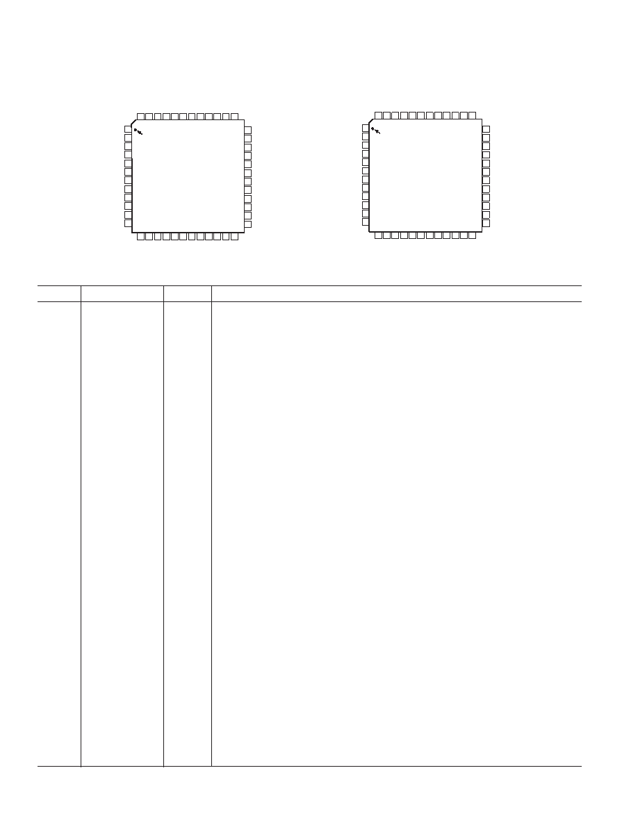
PIN FUNCTION DESCRIPTIONS
Pin
Mnemonic
Type
*
Description
1–5
D0–D4
DO
1–5
D2–D6
DO
Data Outputs AD9849 Only
6
DVSS3
P
Digital Ground 3 – Data Outputs
7
DVDD3
P
Digital Supply 3 – Data Outputs
8–12
D5–D9
DO
Data Outputs (D9 is MSB) AD9848 Only
8–12
D7–D11
DO
Data Outputs (D9 is MSB) AD9849 Only
13, 14
H1, H2
DO
Horizontal Clocks (to CCD)
15
DVSS1
P
Digital Ground 1 – H Drivers
16
DVDD1
P
Digital Supply 1 – H Drivers
17, 18
H3, H4
DO
Horizontal Clocks (to CCD)
19
DVSS2
P
Digital Ground 1 – RG Driver
20
RG
DO
Reset Gate Clock (to CCD)
21
DVDD2
P
Digital Supply 2 – RG Driver
22
AVSS1
P
Analog Ground 1
23
CLI
DI
Master Clock Input
24
AVDD1
P
Analog Supply 1
25
AVSS2
P
Analog Ground 2
26
AVDD2
P
Analog Supply 2
27
BYP1
AO
Bypass Pin (0.1
F to AVSS)
28
BYP2
AO
Bypass Pin (0.1
F to AVSS)
29
CCDIN
AI
Analog Input for CCD Signal
30
BYP3
AO
Bypass Pin (0.1
F to AVSS)
31
AVDD3
P
Analog Supply 3
32
AVSS3
P
Analog Ground 3
33
CMLEVEL
AO
Internal Bias Level Decoupling (0.1
F to AVSS)
34
REFB
AO
Reference Bottom Decoupling (1.0
F to AVSS)
35
REFT
AO
Reference Top Decoupling (1.0
F to AVSS)
36
SL
DI
3-Wire Serial Load (from
P)
37
SDI
DI
3-Wire Serial Data Input (from
P)
38
SCK
DI
3-Wire Serial Clock (from
P)
39
CLPOB
DI
Optical Black Clamp Pulse
40
CLPDM
DI
Dummy Black Clamp Pulse
41
HBLK
DI
HCLK Blanking Pulse
42
PBLK
DI
Preblanking Pulse
43
VD
DI
Vertical Sync Pulse
44
HD
DI
Horizontal Sync Pulse
45
DVSS4
P
Digital Ground 4 – VD, HD, CLPOB, CLPDM, HBLK, PBLK, SCK, SL, SDATA
46
DVDD4
P
Digital Supply 4 – VD, HD, CLPOB, CLPDM, HBLK, PBLK, CK, SL, SDATA
47, 48
NC
Internally Not Connected AD9848 Only
47, 48
D0, D1
DO
Data Output (D0 is LSB) AD9849 Only
*Type: AI = Analog Input, AO = Analog Output, DI = Digital Input, DO = Digital Output, P = Power
PIN CONFIGURATION
相關(guān)PDF資料 |
PDF描述 |
|---|---|
| AD9850BRS | IC DDS DAC W/COMP 125MHZ 28-SSOP |
| AD9851BRS | IC DDS DAC W/COMP 180MHZ 28-SSOP |
| AD9852ASVZ | IC DDS SYNTHESIZER CMOS 80-TQFP |
| AD9854ASTZ | IC DDS QUADRATURE CMOS 80-LQFP |
| AD9858BSVZ | IC DDS DAC 10BIT 1GSPS 100-TQFP |
相關(guān)代理商/技術(shù)參數(shù) |
參數(shù)描述 |
|---|---|
| AD9849KST | 制造商:Rochester Electronics LLC 功能描述:12 BIT 25 MSPS 5V AFE & T - Tape and Reel 制造商:Analog Devices 功能描述: |
| AD9849KSTRL | 制造商:Analog Devices 功能描述:12 BIT 25 MSPS 5V AFE & T - Tape and Reel |
| AD9850 | 制造商:AD 制造商全稱:Analog Devices 功能描述:CMOS, 125 MHz Complete DDS Synthesizer |
| AD9850/CGPCB | 制造商:Analog Devices 功能描述:NCO/DDS, CMOS, 125MHZ COMPLETE DDS SYNTHESIZER - Bulk |
| AD9850/FSPCB | 制造商:Analog Devices 功能描述:EVALUATION BOARD FOR NCO/DDS, CMOS, 125MHZ COMPLETE DDS SYNTHESIZER 制造商:Analog Devices 功能描述:NCO/DDS, CMOS, 125MHZ COMPLETE DDS SYNTHESIZER - Bulk |
發(fā)布緊急采購,3分鐘左右您將得到回復(fù)。