- 您現(xiàn)在的位置:買賣IC網(wǎng) > PDF目錄165343 > AD7467BRT (ANALOG DEVICES INC) 1.8 V, Micro-Power, 8/10/12-Bit ADCs in 6 Lead SOT-23 PDF資料下載
參數(shù)資料
| 型號: | AD7467BRT |
| 廠商: | ANALOG DEVICES INC |
| 元件分類: | ADC |
| 英文描述: | 1.8 V, Micro-Power, 8/10/12-Bit ADCs in 6 Lead SOT-23 |
| 中文描述: | 1-CH 10-BIT SUCCESSIVE APPROXIMATION ADC, SERIAL ACCESS, PDSO6 |
| 封裝: | MO-178AB, SOT-23, 6 PIN |
| 文件頁數(shù): | 6/24頁 |
| 文件大小: | 327K |
| 代理商: | AD7467BRT |
–14–
REV. PrF
PRELIMINARY TECHNICAL DATA
AD7466/AD7467/AD7468
CIRCUIT INFORMATION
The AD7466/AD7467/AD7468 are fast, micro-power, 12-/
10-/8-bit, A/D converters respectively. The parts can be
operated from a +1.6 V to +3.6 V supply. When operated
from any supply voltage within this range, the AD7466/
AD7467/AD7468 is capable of throughput rates of
200kSPS when provided with a 3.4 MHz clock.
The AD7466/AD7467/AD7468 provides the user with an
on-chip Track/Hold, A/D converter, and a serial interface
housed in a tiny 6-lead SOT-23 or 8-lead MSOP package,
which offer the user considerable space saving advantages
over alternative solutions. The serial clock input accesses
data from the part but also provides the clock source for
the successive-approximation A/D converter. The analog
input range is 0 to VDD. An external reference is not
required for the ADC and neither is there a reference on-
chip. The reference for the AD7466/AD7467/AD7468 is
derived from the power supply and thus giving the widest
dynamic input range.
The AD7466/AD7467/AD7468 also features an Automatic
Power-down mode option to allow power saving between
conversions. The Power-down feature is implemented
across the standard serial interface as described in the
Mode of Operation section.
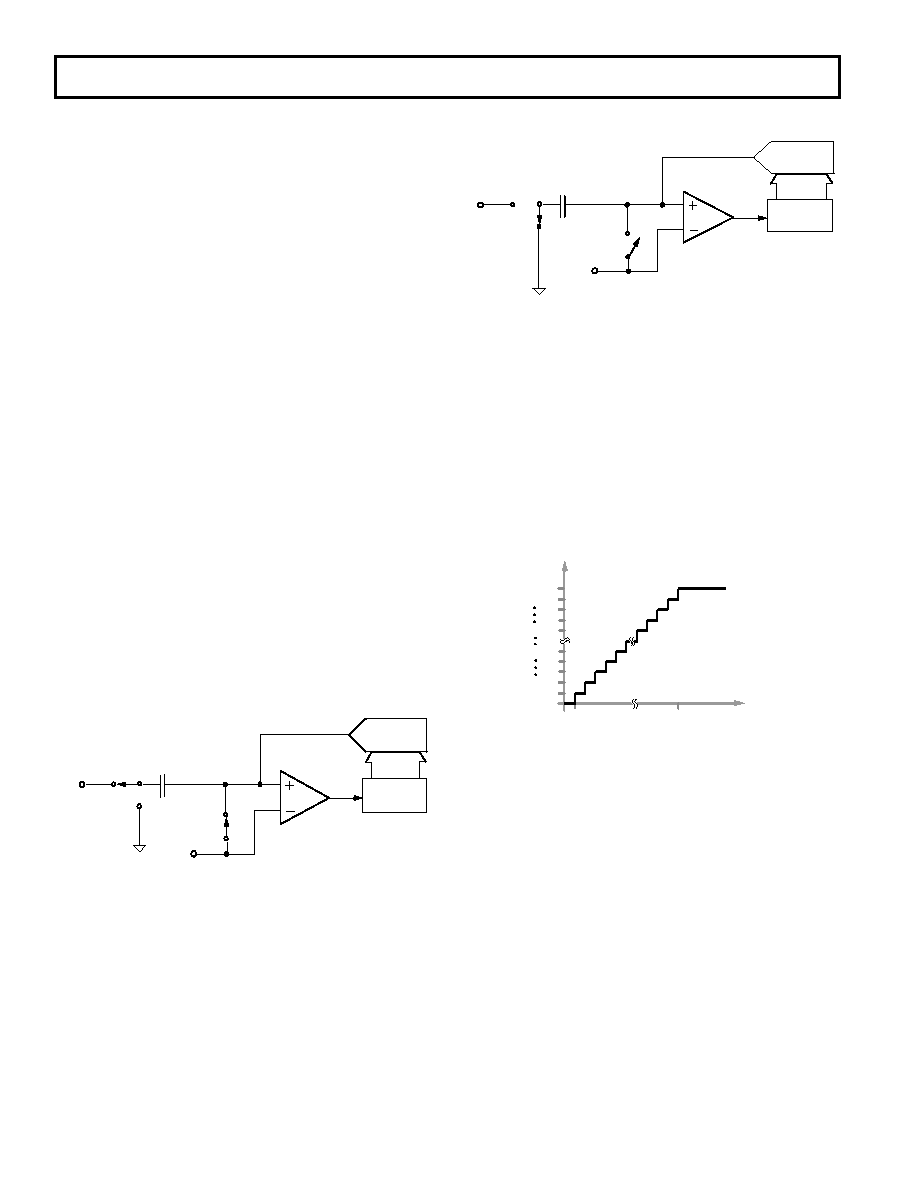
ADC TRANSFER FUNCTION
The output coding of the AD7466/AD7467/AD7468 is
straight binary. The designed code transitions occur at
successive integer LSB values (i.e., 1LSB, 2LSBs, etc.).
The LSB size is VDD/4096 for the AD7466,
VDD/1024
for the AD7467, and
VDD/256 for the AD7468 . The
ideal transfer characteristic for the AD7466/AD7467/
AD7468 is shown in Figure 6.
CONVERTER OPERATION
The AD7466/AD7467/AD7468 is a successive approxi-
mation analog-to-digital converter based around a charge
redistribution DAC. Figures 4 and 5 show simplified
schematics of the ADC. Figure 4 shows the ADC during
its acquisition phase. SW2 is closed and SW1 is in posi-
tion A, the comparator is held in a balanced condition and
the sampling capacitor acquires the signal on VIN.
When the ADC starts a conversion, see Figure 5, SW2
will open and SW1 will move to position B causing the
comparator to become unbalanced. The control logic and
the charge redistribution DAC are used to add and sub-
tract fixed amounts of charge from the sampling capacitor
to bring the comparator back into a balanced condition.
When the comparator is rebalanced the conversion is com-
plete. The control logic generates the ADC output code.
Figure 6 shows the ADC transfer function.
Figure 4. ADC Acquisition Phase
Figure 5. ADC Conversion Phase
Figure 6. AD7466/AD7467/AD7468 Transfer Characteristic
CHARGE
RE DI ST RI B UT I O N
DAC
V IN
V DD /2
SA M PL I N G
CAP ACI T OR
COMP ARAT OR
C ONT RO L
LOG I C
AC QUI SI T I ON
PHASE
SW1
A
B
SW2
AG ND
CHARGE
REDISTRIBUTION
DAC
VIN
VDD /2
SAMPLING
CAPACITOR
COMPARATOR
CONTROL
LOGIC
CONVERSION
PHASE
SW1
A
B
SW2
AGND
000...000
0V
A
D
C
O
D
E
ANALOG INPUT
111...111
000...001
000...010
111...110
111...000
011...111
1LSB
+VDD-1LSB
1LSB = VDD/4096 (AD7466)
1LSB = VDD/1024 (AD7467)
1LSB = VDD/256 (AD7468)
相關(guān)PDF資料 |
PDF描述 |
|---|---|
| AD7468BRT | 1.8 V, Micro-Power, 8/10/12-Bit ADCs in 6 Lead SOT-23 |
| AD7466 | 1.8 V, Micro-Power, 8/10/12-Bit ADCs in 6 Lead SOT-23 |
| AD7467 | 1.8 V, Micro-Power, 8/10/12-Bit ADCs in 6 Lead SOT-23 |
| AD7468 | 1.8 V, Micro-Power, 8/10/12-Bit ADCs in 6 Lead SOT-23 |
| AD746A | Dual Precision, 500 ns Settling, BiFET Op Amp |
相關(guān)代理商/技術(shù)參數(shù) |
參數(shù)描述 |
|---|---|
| AD7467BRT-R | 制造商:AD 制造商全稱:Analog Devices 功能描述:1.6 V, Micropower 12-/10-/8-Bit ADCs |
| AD7467BRT-R2 | 功能描述:IC ADC 10BIT 1.6V LP SOT23-6 RoHS:否 類別:集成電路 (IC) >> 數(shù)據(jù)采集 - 模數(shù)轉(zhuǎn)換器 系列:- 產(chǎn)品培訓(xùn)模塊:Lead (SnPb) Finish for COTS Obsolescence Mitigation Program 標(biāo)準(zhǔn)包裝:2,500 系列:- 位數(shù):12 采樣率(每秒):3M 數(shù)據(jù)接口:- 轉(zhuǎn)換器數(shù)目:- 功率耗散(最大):- 電壓電源:- 工作溫度:- 安裝類型:表面貼裝 封裝/外殼:SOT-23-6 供應(yīng)商設(shè)備封裝:SOT-23-6 包裝:帶卷 (TR) 輸入數(shù)目和類型:- |
| AD7467BRT-REEL | 制造商:AD 制造商全稱:Analog Devices 功能描述:1.6 V, Micropower 12-/10-/8-Bit ADCs |
| AD7467BRT-REEL7 | 制造商:AD 制造商全稱:Analog Devices 功能描述:1.6 V, Micropower 12-/10-/8-Bit ADCs |
| AD7467BRTZ-R | 制造商:AD 制造商全稱:Analog Devices 功能描述:1.6 V, Micropower 12-/10-/8-Bit ADCs |
發(fā)布緊急采購,3分鐘左右您將得到回復(fù)。