- 您現(xiàn)在的位置:買(mǎi)賣(mài)IC網(wǎng) > PDF目錄360656 > 9S12B128DGV1 9S12B128 Device Guide PDF資料下載
參數(shù)資料
| 型號(hào): | 9S12B128DGV1 |
| 英文描述: | 9S12B128 Device Guide |
| 中文描述: | 9S12B128設(shè)備指南 |
| 文件頁(yè)數(shù): | 105/128頁(yè) |
| 文件大?。?/td> | 1823K |
| 代理商: | 9S12B128DGV1 |
第1頁(yè)第2頁(yè)第3頁(yè)第4頁(yè)第5頁(yè)第6頁(yè)第7頁(yè)第8頁(yè)第9頁(yè)第10頁(yè)第11頁(yè)第12頁(yè)第13頁(yè)第14頁(yè)第15頁(yè)第16頁(yè)第17頁(yè)第18頁(yè)第19頁(yè)第20頁(yè)第21頁(yè)第22頁(yè)第23頁(yè)第24頁(yè)第25頁(yè)第26頁(yè)第27頁(yè)第28頁(yè)第29頁(yè)第30頁(yè)第31頁(yè)第32頁(yè)第33頁(yè)第34頁(yè)第35頁(yè)第36頁(yè)第37頁(yè)第38頁(yè)第39頁(yè)第40頁(yè)第41頁(yè)第42頁(yè)第43頁(yè)第44頁(yè)第45頁(yè)第46頁(yè)第47頁(yè)第48頁(yè)第49頁(yè)第50頁(yè)第51頁(yè)第52頁(yè)第53頁(yè)第54頁(yè)第55頁(yè)第56頁(yè)第57頁(yè)第58頁(yè)第59頁(yè)第60頁(yè)第61頁(yè)第62頁(yè)第63頁(yè)第64頁(yè)第65頁(yè)第66頁(yè)第67頁(yè)第68頁(yè)第69頁(yè)第70頁(yè)第71頁(yè)第72頁(yè)第73頁(yè)第74頁(yè)第75頁(yè)第76頁(yè)第77頁(yè)第78頁(yè)第79頁(yè)第80頁(yè)第81頁(yè)第82頁(yè)第83頁(yè)第84頁(yè)第85頁(yè)第86頁(yè)第87頁(yè)第88頁(yè)第89頁(yè)第90頁(yè)第91頁(yè)第92頁(yè)第93頁(yè)第94頁(yè)第95頁(yè)第96頁(yè)第97頁(yè)第98頁(yè)第99頁(yè)第100頁(yè)第101頁(yè)第102頁(yè)第103頁(yè)第104頁(yè)當(dāng)前第105頁(yè)第106頁(yè)第107頁(yè)第108頁(yè)第109頁(yè)第110頁(yè)第111頁(yè)第112頁(yè)第113頁(yè)第114頁(yè)第115頁(yè)第116頁(yè)第117頁(yè)第118頁(yè)第119頁(yè)第120頁(yè)第121頁(yè)第122頁(yè)第123頁(yè)第124頁(yè)第125頁(yè)第126頁(yè)第127頁(yè)第128頁(yè)
Device User Guide —9S12B128DGV1/D V01.11
105
A.5 Reset, Oscillator and PLL
This section summarizes the electrical characteristics of the various startup scenarios for Oscillator and
Phase-Locked-Loop (PLL).
A.5.1 Startup
Table A-19
summarizes several startup characteristics explained in this section. Detailed description of
the startup behavior can be found in the Clock and Reset Generator (CRG) Block User Guide.
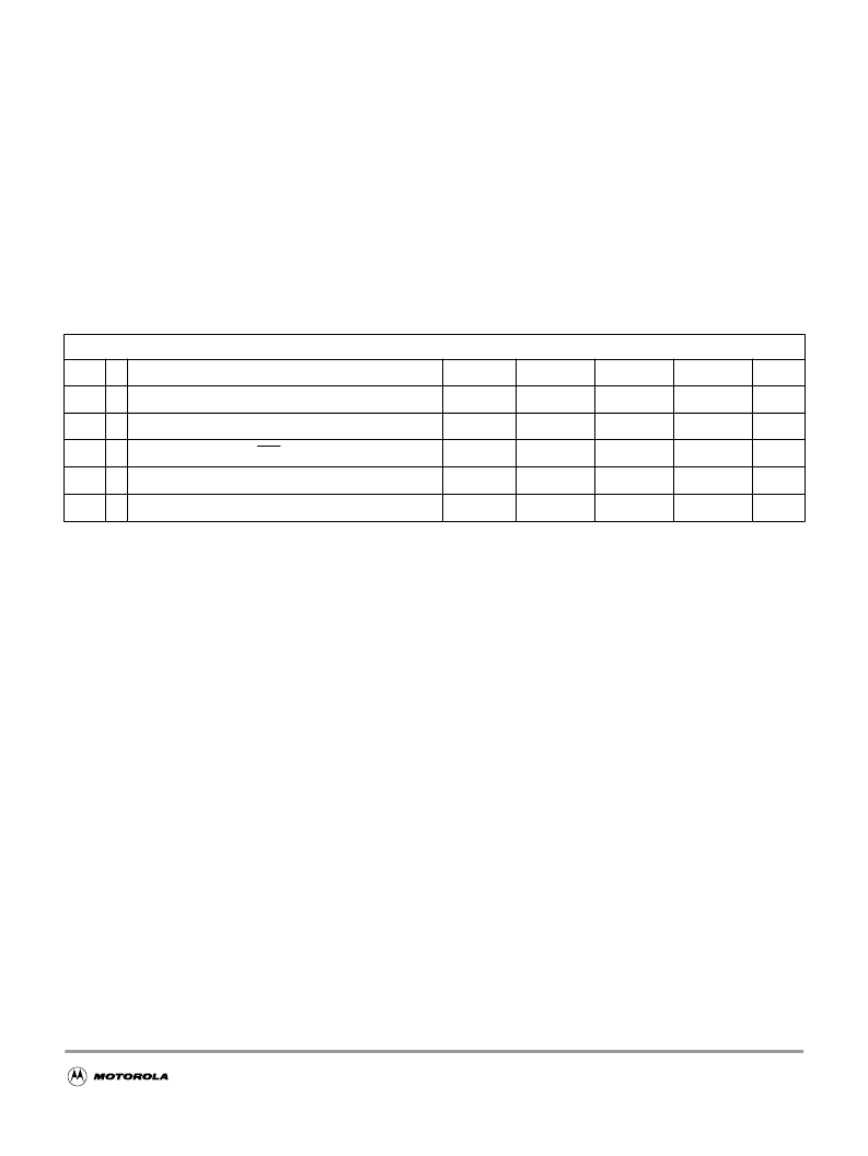
Table A-19 Startup Characteristics
A.5.1.1 POR
ThereleaselevelV
PORD
(see
Table A-17
)andtheassertlevelV
PORA
(see
Table A-17
)arederivedfrom
the V
DD
Supply. They are also valid if the device is powered externally. After releasing the POR reset the
oscillator and the clock quality check are started. If after a time t
CQOUT
no valid oscillation is detected, the
MCU will start using the internal self clock. The fastest startup time possible is given by n
uposc
.
A.5.1.2 LVR
The assert level V
LVRA
(see
Table A-17
) is derived from the V
DD
Supply. After releasing the LVR reset
the oscillator and the clock quality check are started. If after a time t
CQOUT
no valid oscillation is detected,
the MCU will start using the internal self clock. The fastest startup time possible is given by n
uposc
.
A.5.1.3 SRAM Data Retention
Provided an appropriate external reset signal is applied to the MCU, preventing the CPU from executing
codewhenVDD5isoutofspecificationlimits,theSRAMcontentsintegrityisguaranteedifafterthereset
the PORF bit in the CRG Flags Register has not been set.
A.5.1.4 External Reset
When external reset is asserted for a time greater than PW
RSTL
the CRG module generates an internal
reset, and the CPU starts fetching the reset vector without doing a clock quality check, if there was an
oscillation before reset.
Conditions are shown in
Table A-4
unless otherwise noted
Num C
Rating
Symbol
Min
Typ
Max
Unit
1
D Reset input pulse width, minimum input time
PW
RSTL
2
t
osc
2
D Startup from Reset
n
RST
192
196
n
osc
3
D Interrupt pulse width, IRQ edge-sensitive mode
PW
IRQ
20
ns
4
D Wait recovery startup time
t
WRS
14
t
cyc
5
T Voltage Regulator Return from Pseudo Stop
t
vup
100
μ
s
相關(guān)PDF資料 |
PDF描述 |
|---|---|
| 9S12C128DGV1 | MC9S12C Family Device User Guide |
| 9S12D32DGV1 | 9S12DGDJ64DGV1 Device Guide. also covers 9S12D64. 9S12A64. 9S12D32. and 9S12A32 devices |
| 9S12DJ64DGV1 | 9S12DJ64DG Device Guide. also covers 9S12D64. 9S12A64. 9S12D32 and 9S12A32 devices |
| 9S12DJ64-ZIP_PART2 | MC9S12DJ64 Users Guides. zip format. part 2 |
| 9S12DP256BDGV2 | 9S12Dx256B Device Guide. also covers C derivatives and 9S12Ax256 devices |
相關(guān)代理商/技術(shù)參數(shù) |
參數(shù)描述 |
|---|---|
| 9S12C128DGV1 | 制造商:未知廠家 制造商全稱(chēng):未知廠家 功能描述:MC9S12C Family Device User Guide |
| 9S12D32DGV1 | 制造商:未知廠家 制造商全稱(chēng):未知廠家 功能描述:9S12DGDJ64DGV1 Device Guide. also covers 9S12D64. 9S12A64. 9S12D32. and 9S12A32 devices |
| 9S12DJ64DGV1 | 制造商:未知廠家 制造商全稱(chēng):未知廠家 功能描述:9S12DJ64DG Device Guide. also covers 9S12D64. 9S12A64. 9S12D32 and 9S12A32 devices |
| 9S12DP256BDGV1 | 制造商:FREESCALE 制造商全稱(chēng):Freescale Semiconductor, Inc 功能描述:Automotive applications |
| 9S12DP256BDGV2 | 制造商:未知廠家 制造商全稱(chēng):未知廠家 功能描述:9S12Dx256B Device Guide. also covers C derivatives and 9S12Ax256 devices |
發(fā)布緊急采購(gòu),3分鐘左右您將得到回復(fù)。