- 您現(xiàn)在的位置:買賣IC網(wǎng) > PDF目錄24864 > 950812YGT (INTEGRATED DEVICE TECHNOLOGY INC) 200 MHz, PROC SPECIFIC CLOCK GENERATOR, PDSO56 PDF資料下載
參數(shù)資料
| 型號: | 950812YGT |
| 廠商: | INTEGRATED DEVICE TECHNOLOGY INC |
| 元件分類: | 時鐘產(chǎn)生/分配 |
| 英文描述: | 200 MHz, PROC SPECIFIC CLOCK GENERATOR, PDSO56 |
| 封裝: | 6.10 MM, 0.50 MM PITCH, MO-153, TSSOP-56 |
| 文件頁數(shù): | 19/30頁 |
| 文件大小: | 227K |
| 代理商: | 950812YGT |
第1頁第2頁第3頁第4頁第5頁第6頁第7頁第8頁第9頁第10頁第11頁第12頁第13頁第14頁第15頁第16頁第17頁第18頁當(dāng)前第19頁第20頁第21頁第22頁第23頁第24頁第25頁第26頁第27頁第28頁第29頁第30頁
IDTTM Frequency Generator with 200MHz Differential CPU Clocks
0542J—01/25/10
ICS950812
Frequency Generator with 200MHz Differential CPU Clocks
26
PD# Functionality
#
D
PT
K
L
C
U
P
CC
K
L
C
U
P
C6
6
V
3T
U
O
_
z
H
M
6
F
_
K
L
C
I
C
P
K
L
C
I
C
P
K
L
C
I
C
P
T
O
D
/
B
S
U
z
H
M
8
4
1l
a
m
r
o
Nl
a
m
r
o
Nz
H
M
6
6N
I
_
z
H
M
6
2
/
N
I
_
z
H
M
6
62
/
N
I
_
z
H
M
6
z
H
M
8
4
0t
l
u
M
*
f
e
r
it
a
o
l
Fw
o
Lw
o
Lw
o
Lw
o
Lw
o
L
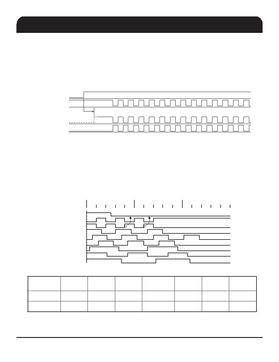
CPU_STOP# - De-assertion (transition from logic "0" to logic "1")
De-assertion of CPU_STOP# Waveforms
All CPU outputs that were stopped are to resume normal operation in a glitch free manner. The maximum latency from the de-
assertion to active outputs is to be defined to be between 2 - 6 CPU clock periods (2 clocks are shown). If the I2C Bit 6 of Byte
1 is programmed to "1" then the stopped CPU outputs will be driven High within 10 nS of CPU_Stop# de-assertion.
When PWRDWN# is sampled low by two consecutive rising edges of CPU clock, then all clock outputs except CPU clocks
must be held low on their next high to low transitions. When the I2C Bit 6 of Byte 0 is programmed to '0' CPU clocks must be
held with the CPU clock pin driven high with a value of 2 x Iref, and CPU# undriven. If Bit 6 of Byte 0 is '1' then both CPU and
CPU# are undriven. Note the example below shows CPU = 133 MHz and Bit 6 of Byte 0 = '0', this diagram and description is
applicable for all valid CPU frequencies 66, 100, 133, 200 MHz.
Due to the state if the internal logic, stopping and holding the REF clock outputs in the LOW state may require more than one
clock cycle to complete.
PD# - Assertion (transition from logic "1" to logic "0")
Power Down Assertion of Waveforms
0ns
PD#
CPUCLKT 100MHz
CPUCLKC 100MHz
3V66MHz
66MHz_IN
66MHz_OUT
PCICLK 33MHz
USB 48MHz
REF 14.318MHz
25ns
50ns
CPU_STOP#
CPUCLKT(2:0)
*CPUCLKT(2:0)TS
CPUCLKC(2:0)
Tdrive_CPU_STOP# <10ns @ 200mV
*Signal TS is CPUCLKT in Tri-State mode
相關(guān)PDF資料 |
PDF描述 |
|---|---|
| 950902DGLFT | 200.4 MHz, PROC SPECIFIC CLOCK GENERATOR, PDSO56 |
| 08056C103JAT7A | Separating plate, width: 0.8 mm, color: gray - TS-GSK |
| 08056C103JAT9A | General Specifications |
| 950902DGLF | 200.4 MHz, PROC SPECIFIC CLOCK GENERATOR, PDSO56 |
| 08056C103KA72A | General Specifications |
相關(guān)代理商/技術(shù)參數(shù) |
參數(shù)描述 |
|---|---|
| 950813 | 制造商:Weidmuller 功能描述:NEXT 74/55/16, 4GP, ST, ZINC -EA - Bulk |
| 9508131 | 制造商:Molex 功能描述: |
| 9508141 | 制造商:Molex 功能描述:Conn Housing RCP 14 POS 3.96mm Crimp ST Bag |
| 9508143 | 制造商:Molex 功能描述: |
| 950815 | 制造商:Weidmuller 功能描述:NEXT 98/74/16, 4GP, ST, ZINC -EA - Bulk |
發(fā)布緊急采購,3分鐘左右您將得到回復(fù)。