- 您現(xiàn)在的位置:買賣IC網(wǎng) > PDF目錄36339 > 935264533557 (NXP SEMICONDUCTORS) SPECIALTY CONSUMER CIRCUIT, PQFP100 PDF資料下載
參數(shù)資料
| 型號: | 935264533557 |
| 廠商: | NXP SEMICONDUCTORS |
| 元件分類: | 消費(fèi)家電 |
| 英文描述: | SPECIALTY CONSUMER CIRCUIT, PQFP100 |
| 封裝: | SOT-317, MQFP-100 |
| 文件頁數(shù): | 43/43頁 |
| 文件大?。?/td> | 254K |
| 代理商: | 935264533557 |
第1頁第2頁第3頁第4頁第5頁第6頁第7頁第8頁第9頁第10頁第11頁第12頁第13頁第14頁第15頁第16頁第17頁第18頁第19頁第20頁第21頁第22頁第23頁第24頁第25頁第26頁第27頁第28頁第29頁第30頁第31頁第32頁第33頁第34頁第35頁第36頁第37頁第38頁第39頁第40頁第41頁第42頁當(dāng)前第43頁
1999 March 01
9
Philips Semiconductors
Product specication
Single chip DVB-C channel receiver
VES1820X
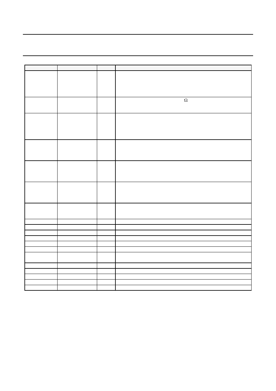
SYMBOL
PIN NUMBER
TYPE
DESCRIPTION
CMCAP
85
I
This pin is connected to a tap point on an internal resistor divider
used to create CMO and CMI. An external capacitor of value 0.1
f
should be connected between this point and ground to provide good
power
supply
rejection
from
the
positive
supply
at
higher
frequencies.
RBIAS
82
I
An external resistor of value 3.3k
should be connected between
this pin and ground to provide good accurate bias currents for the
analog circuits on the ADC.
VREF
88
O
This is the output of an on-chip resistor divider. An external capacitor
of value 0.1
f should be connected between this point and ground to
provide good power supply rejection from the positive supply at
higher frequencies. Reference voltages VREFP and VREFM are
derived from the voltage on VREF.
VREFP
87
O
This is a positive voltage reference for the A/D converter. It is derived
from the voltage on pin VREF through an on-chip fully-differential
amplifier. The voltage on this pin is nominally equal to CMO + 0.25
volts.
VREFM
86
O
This is the negative voltage reference for the A/D converter. It is
derived from the voltage on pin VREF through an on-chip fully-
differential amplifier. The voltage on this pin is nominally equal to
CMO- 0.25 volts.
CMO
84
O
This pin provides the common-mode out voltage for the analog
circuits on the ADC. It is the buffered version of a voltage derived
from an on-chip resistor devider, and has a nominal value of 0.5 x
VD3.
CMI
83
O
This pin provides the common-mode in voltage for the analog circuits
on the ADC. It is the buffered version of a voltage derived from an
on-chip resistor devider, and has a nominal value of 0.75 x VD3.
VD1
81
I
Power supply input for the digital switching circuitry (3.3 typ).
VS1
80
I
Ground return for the digital switching circuitry.
VD2
94
I
Power supply input for the analog clock drivers (3.3V typ).
VS2
93
I
Ground return for the analog clock drivers.
VD3
89
I
Power supply input for the analog circuits (3.3V typ).
VS3
90
I
Ground return for analog circuits.
VD4
95
I
Power supply input that connects to an n-well guard ring that
surrounds the ADC (3.3V typ).
DVCC
96
I
3.3V supply for the digital section of the PLL.
DGND
97
I
Ground connection for the digital section of the PLL.
PLLGND
98
I
Ground connection for the analog section of the PLL.
PLLVCC
99
I
3.3V supply for the analog section of the PLL.
PPLUS
100
I
P-well bias for the analog section of the PLL. Must be tied to 0V.
相關(guān)PDF資料 |
PDF描述 |
|---|---|
| 935264539557 | SPECIALTY CONSUMER CIRCUIT, PQFP100 |
| 935266871557 | SPECIALTY CONSUMER CIRCUIT, PBGA292 |
| 935266917557 | SPECIALTY CONSUMER CIRCUIT, PBGA292 |
| 935268386557 | SPECIALTY CONSUMER CIRCUIT, PBGA292 |
| 935267050025 | SPECIALTY CONSUMER CIRCUIT, UUC |
相關(guān)代理商/技術(shù)參數(shù) |
參數(shù)描述 |
|---|---|
| 935267356112 | 制造商:NXP Semiconductors 功能描述:IC TEA1507PN |
| 935268081112 | 制造商:NXP Semiconductors 功能描述:SUB ONLY IC |
| 935268721125 | 制造商:NXP Semiconductors 功能描述:Buffer/Line Driver 1-CH Non-Inverting 3-ST CMOS 5-Pin TSSOP T/R |
| 935269304128 | 制造商:ST-Ericsson 功能描述:IC AUDIO CODEC W/TCH SCRN 48LQFP |
| 935269544557 | 制造商:NXP Semiconductors 功能描述:SUB ONLY TDA9587-2US1-V1.3 |
發(fā)布緊急采購,3分鐘左右您將得到回復(fù)。