- 您現(xiàn)在的位置:買(mǎi)賣(mài)IC網(wǎng) > PDF目錄24809 > 935263294551 (NXP SEMICONDUCTORS) 2 CHANNEL(S), 1M bps, SERIAL COMM CONTROLLER, PQFP44 PDF資料下載
參數(shù)資料
| 型號(hào): | 935263294551 |
| 廠(chǎng)商: | NXP SEMICONDUCTORS |
| 元件分類(lèi): | 微控制器/微處理器 |
| 英文描述: | 2 CHANNEL(S), 1M bps, SERIAL COMM CONTROLLER, PQFP44 |
| 封裝: | 10 X 10 X 1.75 MM, PLASTIC, QFP-44 |
| 文件頁(yè)數(shù): | 15/48頁(yè) |
| 文件大小: | 324K |
| 代理商: | 935263294551 |
第1頁(yè)第2頁(yè)第3頁(yè)第4頁(yè)第5頁(yè)第6頁(yè)第7頁(yè)第8頁(yè)第9頁(yè)第10頁(yè)第11頁(yè)第12頁(yè)第13頁(yè)第14頁(yè)當(dāng)前第15頁(yè)第16頁(yè)第17頁(yè)第18頁(yè)第19頁(yè)第20頁(yè)第21頁(yè)第22頁(yè)第23頁(yè)第24頁(yè)第25頁(yè)第26頁(yè)第27頁(yè)第28頁(yè)第29頁(yè)第30頁(yè)第31頁(yè)第32頁(yè)第33頁(yè)第34頁(yè)第35頁(yè)第36頁(yè)第37頁(yè)第38頁(yè)第39頁(yè)第40頁(yè)第41頁(yè)第42頁(yè)第43頁(yè)第44頁(yè)第45頁(yè)第46頁(yè)第47頁(yè)第48頁(yè)
Philips Semiconductors
Product specification
SC28L92
3.3V–5.0V Dual Universal Asynchronous
Receiver/Transmitter (DUART)
2000 Jan 21
22
CTPL
– COUNTER TIMER PRESET REGISTER, LOWER
Bits 7:0
8 LSB of the BRG Timer divisor.
ACR
– AUXILIARY CONTROL REGISTER AND CHANGE OF STATE CONTROL
Bit 7
Bit 6:4
Bit 3
Bit 2
Bit 1
Bit 0
Baud Group
Counter Timer mode and clock select
Enable IP3
Enable IP2
Enable IP1
Enable IP0
IPCR
– INPUT PORT CHANGE REGISTER
Bit 7
Bit 6
Bit 5
Bit 4
Bit 3
Bit 2
Bit 1
Bit 0
Delta IP3
Delta IP2
Delta IP1
Delta IP0
State of IP3
State of IP2
State of IP1
State of IP0
IPR
– INPUT PORT REGISTER
Bit 7
Bit 6
Bit 5
Bit 4
Bit 3
Bit 2
Bit 1
Bit 0
State of IP
State of IP 6
State of IP 5
State of IP 4
State of IP 3
State of IP 2
State of IP1
State of IP 0
SOPR – SET THE OUTPUT PORT BITS (OPR)
Bit 7
BIT 6
BIT 5
BIT 4
BIT 3
BIT 2
BIT 1
BIT 0
Set OP 7
Set OP 6
Set OP 5
Set OP 4
Set OP 3
Set OP 2
Set OP 1
Set OP 0
ROPR – RESET OUTPUT PORT BITS (OPR)
Bit 7
BIT 6
BIT 5
BIT 4
BIT 3
BIT 2
BIT 1
BIT 0
Reset OP 7
Reset OP 6
Reset OP 5
Reset OP 4
Reset OP 3
Reset OP 2
Reset OP 1
Reset OP 0
OPCR OUTPUT PORT CONFIGURATION REGISTER (NOTE OP1 AND OP0 ARE THE RTSN OUTPUT AND
ARE CONTROLLED BY THE MR REGISTER)
Bit 7
BIT 6
BIT 5
BIT 4
BIT(3:2)
BIT(1:0)
Configure OP7
Configure OP6
Configure OP5
Configure OP4
Configure OP3
Configure OP2
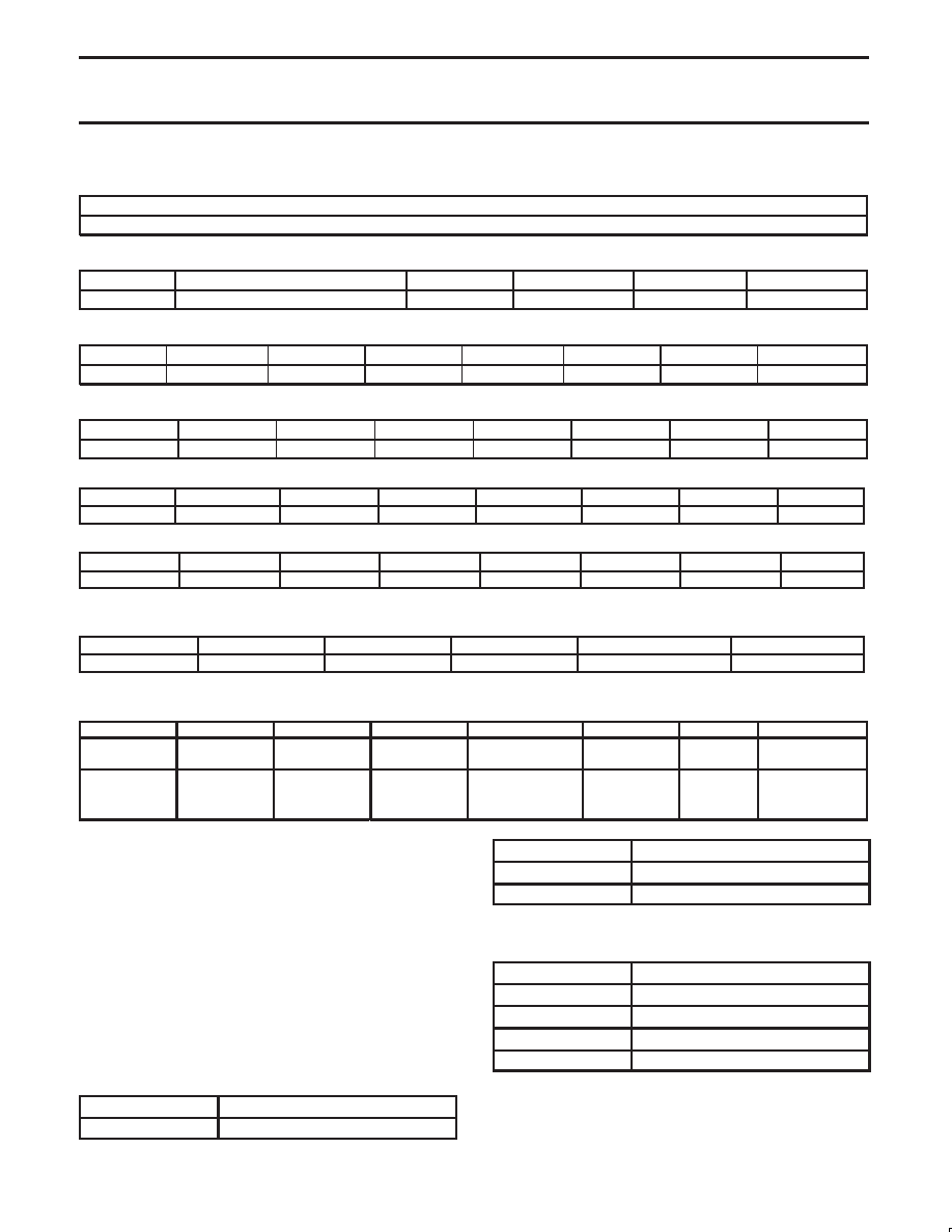
REGISTER DESCRIPTIONS Mode Registers
MR0A Mode Register 0. MR0 is accessed by setting the MR pointer to 0 via the command register command B.
Addr
Bit 7
BIT 6
BITS 5:4
BIT 3
BIT 2
BIT 1
BIT 0
MR0A/
MR0B
Rx
WATCHDOG
RxINT BIT 2
TxINT (1:0)
FIFO SIZE
BAUD RATE
EXTENDED II
TEST 2
BAUD RATE
EXTENDED 1
0x00
0x08
0 = Disable
1 = Enable
See Tables in
MR0
description
See Table 4
0 = 8 byte FIFO
1 = 16 byte FIFO
0 = Normal
1 = Extend II
Set to 0
0 = Normal
1 = Extend
MR0[7]—This bit controls the receiver watch dog timer. 0 = disable,
1 = enable. When enabled, the watch dog timer will generate a
receiver interrupt if the receiver FIFO has not been accessed within
64 bit times of the receiver 1X clock. This is used to alert the control
processor that data is in the RxFIFO that has not been read. This
situation may occur when the byte count of the last part of a
message is not large enough to generate an interrupt.
MR0[6]—Bit 2 of receiver FIFO interrupt level. This bit along with Bit
6 of MR1 sets the fill level of the FIFO that generates the receiver
interrupt.
MR0[6] MR1[6] Note that this control is split between MR0 and
MR1. This is for backward compatibility to the SC2692 and
SCN2681.
Table 3. Receiver FIFO interrupt fill level
(MR0(3) = 0 (8 bytes)
MR0[6] MR1[6]
Interrupt Condition
00
1 or more bytes in FIFO (Rx RDY)
01
3 or more bytes in FIFO
10
6 or more bytes in FIFO
11
8 bytes in FIFO (Rx FULL)
Table 3a. Receiver FIFO interrupt fill
level(MR0(3)=1 (16 bytes)
MR0[6] MR1[6]
Interrupt Condition
00
1 or more bytes in FIFO (Rx RDY)
01
8 or more bytes in FIFO
10
12 or more bytes in FIFO
11
16 bytes in FIFO (Rx FULL)
相關(guān)PDF資料 |
PDF描述 |
|---|---|
| 935263293518 | 2 CHANNEL(S), 1M bps, SERIAL COMM CONTROLLER, PQCC44 |
| 935263294528 | 2 CHANNEL(S), 1M bps, SERIAL COMM CONTROLLER, PQFP44 |
| 07LC-10T050 | ISOLATED DC/DC CONVERTERS 48V Input / 5V/2A or 12V/1A or 24V/0.5A Output |
| 07LC-10T120 | ISOLATED DC/DC CONVERTERS 48V Input / 5V/2A or 12V/1A or 24V/0.5A Output |
| 07LC-10T240 | ISOLATED DC/DC CONVERTERS 48V Input / 5V/2A or 12V/1A or 24V/0.5A Output |
相關(guān)代理商/技術(shù)參數(shù) |
參數(shù)描述 |
|---|---|
| 935264217557 | 制造商:NXP Semiconductors 功能描述:SUB ONLY IC |
| 935267356112 | 制造商:NXP Semiconductors 功能描述:IC TEA1507PN |
| 935268081112 | 制造商:NXP Semiconductors 功能描述:SUB ONLY IC |
| 935268721125 | 制造商:NXP Semiconductors 功能描述:Buffer/Line Driver 1-CH Non-Inverting 3-ST CMOS 5-Pin TSSOP T/R |
| 935269304128 | 制造商:ST-Ericsson 功能描述:IC AUDIO CODEC W/TCH SCRN 48LQFP |
發(fā)布緊急采購(gòu),3分鐘左右您將得到回復(fù)。