- 您現(xiàn)在的位置:買賣IC網(wǎng) > PDF目錄360436 > 74F50109 (NXP Semiconductors N.V.) Synchronizing dual J-K positive edge-triggered flip-flop with metastable immune characteristics PDF資料下載
參數(shù)資料
| 型號(hào): | 74F50109 |
| 廠商: | NXP Semiconductors N.V. |
| 英文描述: | Synchronizing dual J-K positive edge-triggered flip-flop with metastable immune characteristics |
| 中文描述: | 同步雙JK正沿觸發(fā)器與亞穩(wěn)態(tài)觸發(fā)器免疫特性 |
| 文件頁(yè)數(shù): | 6/12頁(yè) |
| 文件大小: | 97K |
| 代理商: | 74F50109 |
Philips Semiconductors
Product specification
74F50109
Synchronizing dual J–K positive edge-triggered
flip-flop with metastable immune characteristics
September 14, 1990
6
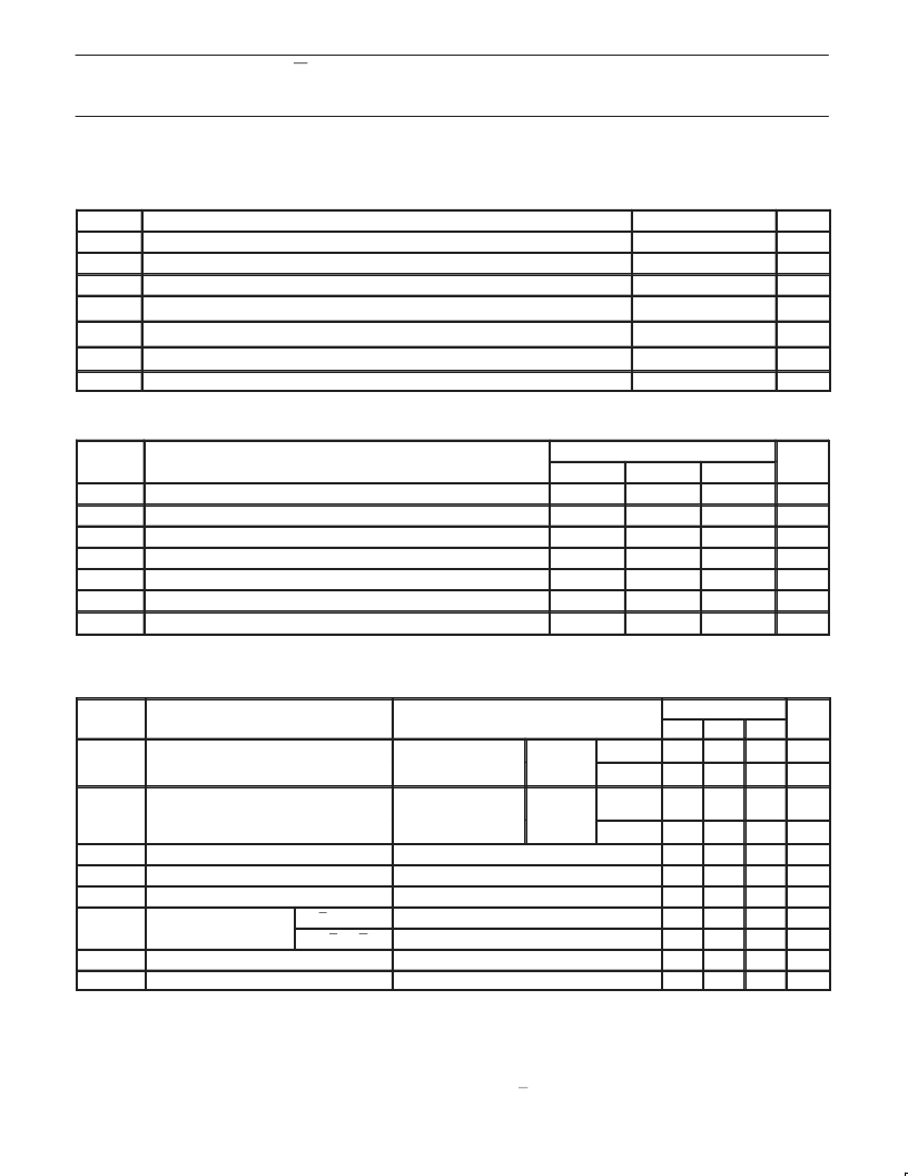
ABSOLUTE MAXIMUM RATINGS
(Operation beyond the limit set forth in this table may impair the useful life of the device. Unless otherwise noted these limits are over the
operating free air temperature range.)
SYMBOL
PARAMETER
RATING
UNIT
V
CC
V
IN
I
IN
V
OUT
Supply voltage
–0.5 to +7.0
V
Input voltage
–0.5 to +7.0
V
Input current
–30 to +5
mA
Voltage applied to output in high output state
–0.5 to V
CC
V
I
OUT
Current applied to output in low output state
40
mA
T
amb
Operating free air temperature range
0 to +70
°
C
°
C
T
stg
Storage temperature range
–65 to +150
RECOMMENDED OPERATING CONDITIONS
SYMBOL
PARAMETER
LIMITS
UNIT
MIN
NOM
MAX
V
CC
V
IH
V
IL
I
Ik
I
OH
I
OL
Supply voltage
4.5
5.0
5.5
V
High–level input voltage
2.0
V
Low–level input voltage
0.8
V
Input clamp current
–18
mA
High–level output current
–1
mA
Low–level output current
20
mA
°
C
T
amb
Operating free air temperature range
0
+70
DC ELECTRICAL CHARACTERISTICS
(Over recommended operating free-air temperature range unless otherwise noted.)
SYMBOL
PARAMETER
TEST
LIMITS
TYP
2
UNIT
CONDITIONS
1
MIN
MAX
V
OH
High–level output voltage
V
= MIN, V
IL
=
MAX,
V
IH
= MIN
I
OH
= MAX
±
10%V
CC
±
5%V
CC
2.5
V
2.7
3.4
V
V
OL
Low–level output voltage
V
= MIN, V
IL
=
MAX,
I
OL
= MAX
±
10%V
CC
0.30
0.50
V
V
IH
= MIN
±
5%V
CC
0.30
0.50
V
V
IK
I
I
I
IH
I
IL
Input clamp voltage
V
CC
= MIN, I
I
= I
IK
V
CC
= MAX, V
I
= 7.0V
V
CC
= MAX, V
I
= 2.7V
V
CC
= MAX, V
I
= 0.5V
V
CC
= MAX, V
I
= 0.5V
V
CC
= MAX
V
CC
= MAX
-0.73
-1.2
V
Input current at maximum input voltage
100
μ
A
μ
A
μ
A
μ
A
High–level input current
20
Low–level input current
Jn, Kn
-250
CPn, SDn, RDn
-20
I
OS
I
CC
Short circuit output current
3
Supply current
4
(total)
-60
-150
mA
22
32
mA
NOTES:
1. For conditions shown as MIN or MAX, use the appropriate value specified under recommended operating conditions for the applicable type.
2. All typical values are at V
CC
= 5V, T
amb
= 25
°
C.
3. Not more than one output should be shorted at a time. For testing I
OS
, the use of high-speed test apparatus and/or sample-and-hold
techniques are preferable in order to minimize internal heating and more accurately reflect operational values. Otherwise, prolonged shorting
of a high output may raise the chip temperature well above normal and thereby cause invalid readings in other parameter tests. In any
sequence of parameter tests, I
OS
tests should be performed last.
4. Measure I
CC
with the clock input grounded and all outputs open, then with Q and Q outputs high in turn.
相關(guān)PDF資料 |
PDF描述 |
|---|---|
| 74F597 | 8-bit shift register with input storage registers(帶輸入存儲(chǔ)寄存的8位移位寄存器(三態(tài))) |
| 74F50728 | Synchronizing cascaded dual positive edge-triggered D-type flip-flop |
| 74F50729 | Synchronizing dual D-type flip-flop with edge-triggered set and reset with metastable immune characteristics |
| 74F5074 | Synchronizing dual D-type flip-flop/clock driver(同步雙D觸發(fā)器/時(shí)鐘驅(qū)動(dòng)器) |
| 74F51SCX | 2/2-input and 3/3-input AND-NOR Gate |
相關(guān)代理商/技術(shù)參數(shù) |
參數(shù)描述 |
|---|---|
| 74F50728 | 制造商:PHILIPS 制造商全稱:NXP Semiconductors 功能描述:Synchronizing cascaded dual positive edge-triggered D-type flip-flop |
| 74F50729 | 制造商:PHILIPS 制造商全稱:NXP Semiconductors 功能描述:Synchronizing dual D-type flip-flop with edge-triggered set and reset with metastable immune characteristics |
| 74F5074 | 制造商:PHILIPS 制造商全稱:NXP Semiconductors 功能描述:Synchronizing dual D-type flip-flop/clock driver |
| 74F5074D | 制造商:SGS 功能描述:74F5074 SGS S1I2B 制造商:NXP Semiconductors 功能描述: |
| 74F5074N | 制造商:NXP Semiconductors 功能描述: |
發(fā)布緊急采購(gòu),3分鐘左右您將得到回復(fù)。