- 您現(xiàn)在的位置:買(mǎi)賣(mài)IC網(wǎng) > PDF目錄4291 > XC2S100E-6TQG144C (Xilinx Inc)IC FPGA 1.8V 600 CLB'S 144-TQFP PDF資料下載
參數(shù)資料
| 型號(hào): | XC2S100E-6TQG144C |
| 廠商: | Xilinx Inc |
| 文件頁(yè)數(shù): | 2/108頁(yè) |
| 文件大?。?/td> | 0K |
| 描述: | IC FPGA 1.8V 600 CLB'S 144-TQFP |
| 產(chǎn)品變化通告: | FPGA Family Discontinuation 18/Apr/2011 |
| 標(biāo)準(zhǔn)包裝: | 60 |
| 系列: | Spartan®-IIE |
| LAB/CLB數(shù): | 600 |
| 邏輯元件/單元數(shù): | 2700 |
| RAM 位總計(jì): | 40960 |
| 輸入/輸出數(shù): | 102 |
| 門(mén)數(shù): | 100000 |
| 電源電壓: | 1.71 V ~ 1.89 V |
| 安裝類(lèi)型: | 表面貼裝 |
| 工作溫度: | 0°C ~ 85°C |
| 封裝/外殼: | 144-LQFP |
| 供應(yīng)商設(shè)備封裝: | 144-TQFP(20x20) |
| 其它名稱: | 122-1462 |
第1頁(yè)當(dāng)前第2頁(yè)第3頁(yè)第4頁(yè)第5頁(yè)第6頁(yè)第7頁(yè)第8頁(yè)第9頁(yè)第10頁(yè)第11頁(yè)第12頁(yè)第13頁(yè)第14頁(yè)第15頁(yè)第16頁(yè)第17頁(yè)第18頁(yè)第19頁(yè)第20頁(yè)第21頁(yè)第22頁(yè)第23頁(yè)第24頁(yè)第25頁(yè)第26頁(yè)第27頁(yè)第28頁(yè)第29頁(yè)第30頁(yè)第31頁(yè)第32頁(yè)第33頁(yè)第34頁(yè)第35頁(yè)第36頁(yè)第37頁(yè)第38頁(yè)第39頁(yè)第40頁(yè)第41頁(yè)第42頁(yè)第43頁(yè)第44頁(yè)第45頁(yè)第46頁(yè)第47頁(yè)第48頁(yè)第49頁(yè)第50頁(yè)第51頁(yè)第52頁(yè)第53頁(yè)第54頁(yè)第55頁(yè)第56頁(yè)第57頁(yè)第58頁(yè)第59頁(yè)第60頁(yè)第61頁(yè)第62頁(yè)第63頁(yè)第64頁(yè)第65頁(yè)第66頁(yè)第67頁(yè)第68頁(yè)第69頁(yè)第70頁(yè)第71頁(yè)第72頁(yè)第73頁(yè)第74頁(yè)第75頁(yè)第76頁(yè)第77頁(yè)第78頁(yè)第79頁(yè)第80頁(yè)第81頁(yè)第82頁(yè)第83頁(yè)第84頁(yè)第85頁(yè)第86頁(yè)第87頁(yè)第88頁(yè)第89頁(yè)第90頁(yè)第91頁(yè)第92頁(yè)第93頁(yè)第94頁(yè)第95頁(yè)第96頁(yè)第97頁(yè)第98頁(yè)第99頁(yè)第100頁(yè)第101頁(yè)第102頁(yè)第103頁(yè)第104頁(yè)第105頁(yè)第106頁(yè)第107頁(yè)第108頁(yè)
10
DS077-2 (v3.0) August 9, 2013
Product Specification
Spartan-IIE FPGA Family: Functional Description
R
— OBSOLETE — OBSOLETE — OBSOLETE — OBSOLETE —
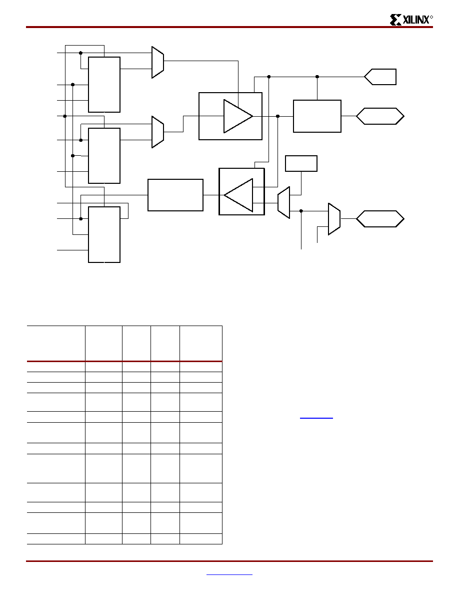
Input/Output Block
The Spartan-IIE FPGA IOB, as seen in Figure 4, features
inputs and outputs that support a wide variety of I/O signal-
ing standards. These high-speed inputs and outputs are
capable of supporting various state of the art memory and
bus interfaces. The default standard is LVTTL. Table 3 lists
several of the standards which are supported along with the
required reference (VREF), output (VCCO) and board termi-
nation (VTT) voltages needed to meet the standard. For
more details on the I/O standards and termination applica-
tion examples, see XAPP179, "Using SelectIO Interfaces in
Spartan-II and Spartan-IIE FPGAs."
The three IOB registers function either as edge-triggered
D-type flip-flops or as level-sensitive latches. Each IOB has
a clock signal (CLK) shared by the three registers and inde-
pendent Clock Enable (CE) signals for each register.
In addition to the CLK and CE control signals, the three reg-
isters share a Set/Reset (SR). For each register, this signal
can be independently configured as a synchronous Set, a
synchronous Reset, an asynchronous Preset, or an asyn-
chronous Clear.
A feature not shown in the block diagram, but controlled by
the software, is polarity control. The input and output buffers
and all of the IOB control signals have independent polarity
controls.
Figure 4: Spartan-IIE Input/Output Block (IOB)
Package Pin
Package
Pin
Package Pin
D
CK
EC
SR
Q
D
CK
EC
SR
Q
D
CK
EC
SR
Q
Programmable
Bias and
ESD Network
VCCO
I/O
I/O, VREF
Internal
Reference
To Next I/O
To Other
External VREF Inputs
of Bank
Notes:
1. For some I/O standards.
Programmable
Input Buffer
Programmable
Output Buffer
Programmable
Delay
VCC
VCC(1)
OE
SR
O
OCE
I
ICE
IQ
CLK
TCE
T
DS077-2_01_051501
TFF
OFF
IFF
Table 3: Standards Supported by I/O (Typical Values)
I/O Standard
Input
Reference
Voltage
(VREF)
Input
Voltage
(VCCO)
Output
Source
Voltage
(VCCO)
Board
Termination
Voltage
(VTT)
LVTTL (2-24 mA)
N/A
3.3
N/A
LVCMOS2
N/A
2.5
N/A
LVCMOS18
N/A
1.8
N/A
PCI (3V,
33 MHz/66 MHz)
N/A
3.3
N/A
GTL
0.8
N/A
1.2
GTL+
1.0
N/A
1.5
HSTL Class I
0.75
N/A
1.5
0.75
HSTL Class III
0.9
N/A
1.5
HSTL Class IV
0.9
N/A
1.5
SSTL3 Class I
and II
1.5
N/A
3.3
1.5
SSTL2 Class I
and II
1.25
N/A
2.5
1.25
CTT
1.5
N/A
3.3
1.5
AGP
1.32
N/A
3.3
N/A
LVDS, Bus LVDS
N/A
2.5
N/A
LVPECL
N/A
3.3
N/A
相關(guān)PDF資料 |
PDF描述 |
|---|---|
| XC2S100E-6TQ144C | IC FPGA 1.8V 600 CLB'S 144-TQFP |
| XA3S200-4PQG208I | IC FPGA SPARTAN-3 200K 208-PQFP |
| 24FC64FT-I/SN | IC EEPROM 64KBIT 1MHZ 8SOIC |
| XA2S50E-6TQ144Q | IC FPGA SPARTAN-IIE 144TQFP |
| RSA50DTBD-S664 | CONN EDGECARD 100PS R/A .125 SLD |
相關(guān)代理商/技術(shù)參數(shù) |
參數(shù)描述 |
|---|---|
| XC2S100E-6TQG144I | 制造商:XILINX 制造商全稱:XILINX 功能描述:Spartan-IIE FPGA |
| XC2S100E7FG456C | 制造商:Xilinx 功能描述: |
| XC2S100E-7FG456C | 制造商:XILINX 制造商全稱:XILINX 功能描述:Spartan-IIE 1.8V FPGA Family |
| XC2S100E-7FG456I | 制造商:XILINX 制造商全稱:XILINX 功能描述:Spartan-IIE 1.8V FPGA Family |
| XC2S100E-7FG676C | 制造商:XILINX 制造商全稱:XILINX 功能描述:Spartan-IIE FPGA |
發(fā)布緊急采購(gòu),3分鐘左右您將得到回復(fù)。