- 您現(xiàn)在的位置:買賣IC網(wǎng) > PDF目錄1973 > XAM1808AZCE4 (Texas Instruments)IC ARM PROCESSOR 361NFBGA PDF資料下載
參數(shù)資料
| 型號(hào): | XAM1808AZCE4 |
| 廠商: | Texas Instruments |
| 文件頁(yè)數(shù): | 65/264頁(yè) |
| 文件大小: | 0K |
| 描述: | IC ARM PROCESSOR 361NFBGA |
| 標(biāo)準(zhǔn)包裝: | 160 |
| 系列: | Sitara ARM®, Cortex™A8 |
| 處理器類型: | ARM 微處理器 |
| 速度: | 456MHz |
| 電壓: | 1.25 V ~ 1.35 V |
| 安裝類型: | 表面貼裝 |
| 封裝/外殼: | 361-LFBGA |
| 供應(yīng)商設(shè)備封裝: | 361-NFBGA(13x13) |
| 包裝: | 托盤 |
| 其它名稱: | 296-27534 XAM1808AZCE4-ND |
第1頁(yè)第2頁(yè)第3頁(yè)第4頁(yè)第5頁(yè)第6頁(yè)第7頁(yè)第8頁(yè)第9頁(yè)第10頁(yè)第11頁(yè)第12頁(yè)第13頁(yè)第14頁(yè)第15頁(yè)第16頁(yè)第17頁(yè)第18頁(yè)第19頁(yè)第20頁(yè)第21頁(yè)第22頁(yè)第23頁(yè)第24頁(yè)第25頁(yè)第26頁(yè)第27頁(yè)第28頁(yè)第29頁(yè)第30頁(yè)第31頁(yè)第32頁(yè)第33頁(yè)第34頁(yè)第35頁(yè)第36頁(yè)第37頁(yè)第38頁(yè)第39頁(yè)第40頁(yè)第41頁(yè)第42頁(yè)第43頁(yè)第44頁(yè)第45頁(yè)第46頁(yè)第47頁(yè)第48頁(yè)第49頁(yè)第50頁(yè)第51頁(yè)第52頁(yè)第53頁(yè)第54頁(yè)第55頁(yè)第56頁(yè)第57頁(yè)第58頁(yè)第59頁(yè)第60頁(yè)第61頁(yè)第62頁(yè)第63頁(yè)第64頁(yè)當(dāng)前第65頁(yè)第66頁(yè)第67頁(yè)第68頁(yè)第69頁(yè)第70頁(yè)第71頁(yè)第72頁(yè)第73頁(yè)第74頁(yè)第75頁(yè)第76頁(yè)第77頁(yè)第78頁(yè)第79頁(yè)第80頁(yè)第81頁(yè)第82頁(yè)第83頁(yè)第84頁(yè)第85頁(yè)第86頁(yè)第87頁(yè)第88頁(yè)第89頁(yè)第90頁(yè)第91頁(yè)第92頁(yè)第93頁(yè)第94頁(yè)第95頁(yè)第96頁(yè)第97頁(yè)第98頁(yè)第99頁(yè)第100頁(yè)第101頁(yè)第102頁(yè)第103頁(yè)第104頁(yè)第105頁(yè)第106頁(yè)第107頁(yè)第108頁(yè)第109頁(yè)第110頁(yè)第111頁(yè)第112頁(yè)第113頁(yè)第114頁(yè)第115頁(yè)第116頁(yè)第117頁(yè)第118頁(yè)第119頁(yè)第120頁(yè)第121頁(yè)第122頁(yè)第123頁(yè)第124頁(yè)第125頁(yè)第126頁(yè)第127頁(yè)第128頁(yè)第129頁(yè)第130頁(yè)第131頁(yè)第132頁(yè)第133頁(yè)第134頁(yè)第135頁(yè)第136頁(yè)第137頁(yè)第138頁(yè)第139頁(yè)第140頁(yè)第141頁(yè)第142頁(yè)第143頁(yè)第144頁(yè)第145頁(yè)第146頁(yè)第147頁(yè)第148頁(yè)第149頁(yè)第150頁(yè)第151頁(yè)第152頁(yè)第153頁(yè)第154頁(yè)第155頁(yè)第156頁(yè)第157頁(yè)第158頁(yè)第159頁(yè)第160頁(yè)第161頁(yè)第162頁(yè)第163頁(yè)第164頁(yè)第165頁(yè)第166頁(yè)第167頁(yè)第168頁(yè)第169頁(yè)第170頁(yè)第171頁(yè)第172頁(yè)第173頁(yè)第174頁(yè)第175頁(yè)第176頁(yè)第177頁(yè)第178頁(yè)第179頁(yè)第180頁(yè)第181頁(yè)第182頁(yè)第183頁(yè)第184頁(yè)第185頁(yè)第186頁(yè)第187頁(yè)第188頁(yè)第189頁(yè)第190頁(yè)第191頁(yè)第192頁(yè)第193頁(yè)第194頁(yè)第195頁(yè)第196頁(yè)第197頁(yè)第198頁(yè)第199頁(yè)第200頁(yè)第201頁(yè)第202頁(yè)第203頁(yè)第204頁(yè)第205頁(yè)第206頁(yè)第207頁(yè)第208頁(yè)第209頁(yè)第210頁(yè)第211頁(yè)第212頁(yè)第213頁(yè)第214頁(yè)第215頁(yè)第216頁(yè)第217頁(yè)第218頁(yè)第219頁(yè)第220頁(yè)第221頁(yè)第222頁(yè)第223頁(yè)第224頁(yè)第225頁(yè)第226頁(yè)第227頁(yè)第228頁(yè)第229頁(yè)第230頁(yè)第231頁(yè)第232頁(yè)第233頁(yè)第234頁(yè)第235頁(yè)第236頁(yè)第237頁(yè)第238頁(yè)第239頁(yè)第240頁(yè)第241頁(yè)第242頁(yè)第243頁(yè)第244頁(yè)第245頁(yè)第246頁(yè)第247頁(yè)第248頁(yè)第249頁(yè)第250頁(yè)第251頁(yè)第252頁(yè)第253頁(yè)第254頁(yè)第255頁(yè)第256頁(yè)第257頁(yè)第258頁(yè)第259頁(yè)第260頁(yè)第261頁(yè)第262頁(yè)第263頁(yè)第264頁(yè)
SPRS653E – FEBRUARY 2010 – REVISED MARCH 2014
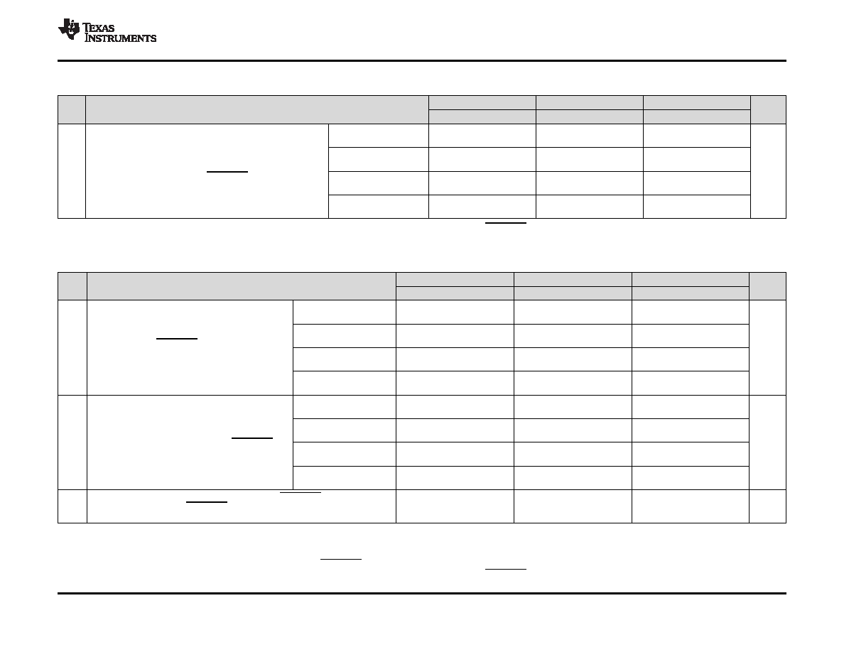
Table 6-67. Additional SPI0 Master Timings, 4-Pin Chip Select Option (1)(2)(3) (continued)
1.3V, 1.2V
1.1V
1.0V
NO.
PARAMETER
UNIT
MIN
MAX
MIN
MAX
MIN
MAX
Polarity = 0, Phase = 0,
0.5M+P-1
0.5M+P-2
0.5M+P-3
from SPI0_CLK falling
Polarity = 0, Phase = 1,
P-1
P-2
P-3
from SPI0_CLK falling
Delay from final SPI0_CLK edge to master
20
td(SPC_SCS)M
ns
deasserting SPI0_SCS (6) (7)
Polarity = 1, Phase = 0,
0.5M+P-1
0.5M+P-2
0.5M+P-3
from SPI0_CLK rising
Polarity = 1, Phase = 1,
P-1
P-2
P-3
from SPI0_CLK rising
(6)
Except for modes when SPIDAT1.CSHOLD is enabled and there is additional data to transmit. In this case, SPI0_SCS will remain asserted.
(7)
This delay can be increased under software control by the register bit field SPIDELAY.T2CDELAY[4:0].
Table 6-68. Additional SPI0 Master Timings, 5-Pin Option (1)(2)(3)
1.3V, 1.2V
1.1V
1.0V
NO.
PARAMETER
UNIT
MIN
MAX
MIN
MAX
MIN
MAX
Polarity = 0, Phase = 0,
0.5M+P+5
0.5M+P+6
from SPI0_CLK falling
Polarity = 0, Phase = 1,
Max delay for slave to deassert
P+5
P+6
from SPI0_CLK falling
SPI0_ENA after final SPI0_CLK
18
td(SPC_ENA)M
ns
edge to ensure master does not
Polarity = 1, Phase = 0,
0.5M+P+5
0.5M+P+6
begin the next transfer.(4)
from SPI0_CLK rising
Polarity = 1, Phase = 1,
P+5
P+6
from SPI0_CLK rising
Polarity = 0, Phase = 0,
0.5M+P-2
0.5M+P-3
from SPI0_CLK falling
Polarity = 0, Phase = 1,
P-2
P-3
Delay from final SPI0_CLK edge to from SPI0_CLK falling
20
td(SPC_SCS)M
master deasserting SPI0_SCS (5)
ns
Polarity = 1, Phase = 0,
(6)
0.5M+P-2
0.5M+P-3
from SPI0_CLK rising
Polarity = 1, Phase = 1,
P-2
P-3
from SPI0_CLK rising
Max delay for slave SPI to drive SPI0_ENA valid after master
21
td(SCSL_ENAL)M
asserts SPI0_SCS to delay the master from beginning the
C2TDELAY+P
ns
next transfer,
(1)
These parameters are in addition to the general timings for SPI master modes (Table 6-65).
(2)
P = SYSCLK2 period; M = tc(SPC)M (SPI master bit clock period)
(3)
Figure shows only Polarity = 0, Phase = 0 as an example. Table gives parameters for all four master clocking modes.
(4)
In the case where the master SPI is ready with new data before SPI0_ENA deassertion.
(5)
Except for modes when SPIDAT1.CSHOLD is enabled and there is additional data to transmit. In this case, SPI0_SCS will remain asserted.
(6)
This delay can be increased under software control by the register bit field SPIDELAY.T2CDELAY[4:0].
Copyright 2010–2014, Texas Instruments Incorporated
Peripheral Information and Electrical Specifications
157
Product Folder Links: AM1808
相關(guān)PDF資料 |
PDF描述 |
|---|---|
| XC1765ESOG8C | IC PROM SERIAL 65K 8-SOIC |
| XC17S200AVQ44I | IC PROM SER 200000 I-TEMP 44VQFP |
| XC17S30XLVOG8I | IC PROM SERIAL 3.3V 300K 8-SOIC |
| XC17V08VQ44I | IC PROM SER I-TEMP 3.3V 44-VQFP |
| XC18V04PCG44C | IC PROM REPROGR 4MB 44-PLCC |
相關(guān)代理商/技術(shù)參數(shù) |
參數(shù)描述 |
|---|---|
| XAM1808AZCEA3 | 制造商:TI 制造商全稱:Texas Instruments 功能描述:AM1808 ARM Microprocessor |
| XAM1808AZCEA4 | 制造商:TI 制造商全稱:Texas Instruments 功能描述:AM1808 ARM Microprocessor |
| XAM1808AZCED3 | 制造商:TI 制造商全稱:Texas Instruments 功能描述:AM1808 ARM Microprocessor |
| XAM1808AZCED4 | 制造商:TI 制造商全稱:Texas Instruments 功能描述:AM1808 ARM Microprocessor |
| XAM1808AZWT3 | 制造商:Texas Instruments 功能描述:ARM MICROPROCESSOR - Tape and Reel |
發(fā)布緊急采購(gòu),3分鐘左右您將得到回復(fù)。