- 您現(xiàn)在的位置:買賣IC網(wǎng) > PDF目錄245706 > WSE128K16-42G2TMA (MICROSEMI CORP-PMG MICROELECTRONICS) SPECIALTY MEMORY CIRCUIT, CQMA68 PDF資料下載
參數(shù)資料
| 型號: | WSE128K16-42G2TMA |
| 廠商: | MICROSEMI CORP-PMG MICROELECTRONICS |
| 元件分類: | 存儲器 |
| 英文描述: | SPECIALTY MEMORY CIRCUIT, CQMA68 |
| 封裝: | CERAMIC, QFP-68 |
| 文件頁數(shù): | 2/15頁 |
| 文件大小: | 635K |
| 代理商: | WSE128K16-42G2TMA |
WSE128K16-XXX
10
White Electronic Designs Corporation (602) 437-1520 www.whiteedc.com
White Electronic Designs
PRELIMINARY
White Electronic Designs Corp. reserves the right to change products or specications without notice.
March 2005
Rev. 3
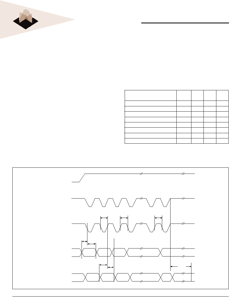
EEPROM PAGE WRITE OPERATION
The WSE128K16-XXX has a page write operation
that allows one to 128 bytes of data to be written into
the device and consecutively loads during the internal
programming period. Successive bytes may be loaded
in the same manner after the rst data byte has been
loaded. An internal timer begins a time out operation at
each write cycle. If another write cycle is completed within
150μs or less, a new time out period begins. Each write
cycle restarts the delay period. The write cycles can be
continued as long as the interval is less than the time out
period.
The usual procedure is to increment the least signicant
address lines from A0 through A6 at each write cycle. In
this manner a page of up to 128 bytes can be loaded in
to the EEPROM in a burst mode before beginning the
relatively long interval programming cycle.
FIGURE 11 – EEPROM PAGE MODE WRITE WAVEFORMS
EEPROM PAGE WRITE CHARACTERISTICS
VCC = 5.0V, GND = 0V, -55°C ≤ TA ≤ +125°C
Page Mode Write Characteristics
Parameter
Symbol
Min
Max
Unit
Write Cycle Time, TYP = 6ms
tWC
10
ms
Address Set-up Time
tAS
0ns
Address Hold Time (1)
tAH
100
ns
Data Set-up Time
tDS
100
ns
Data Hold Time
tDH
10
ns
Write Pulse Width
tWP
150
ns
Byte Load Cycle Time
tBLC
150
μs
Write Pulse Width High
tWPH
50
ns
NOTE:
1. Page address must remain valid for duration of write cycle.
BYTE 0 BYTE 1
BYTE 2
BYTE 3
VALID
DATA
VALID
ADDRESS
tWC
tBLC
tWPH
tWP
BYTE 127
tDS tDH
tAS
tAH
OE#
ECS#1-2
EWE#1-2
ADDRESS
EEPROM
DATA
After the 150μs time out is completed, the EEPROM
begins an internal write cycle. During this cycle the entire
page of bytes will be written at the same time. The internal
programming cycle is the same regardless of the number
of bytes accessed.
相關(guān)PDF資料 |
PDF描述 |
|---|---|
| WED2ZL362MS30BC | 2M X 36 MULTI DEVICE SRAM MODULE, 3 ns, PBGA119 |
| WS128K32L-25G2UM | 128K X 32 MULTI DEVICE SRAM MODULE, 25 ns, CQFP68 |
| W3H64M72E-SBM | 64M X 72 DDR DRAM, PBGA208 |
| WF4M8-150OPC5 | 4M X 8 FLASH 5V PROM, 150 ns, CDSO56 |
| WS128K32V-20HS | 512K X 8 MULTI DEVICE SRAM MODULE, 20 ns, HIP66 |
相關(guān)代理商/技術(shù)參數(shù) |
參數(shù)描述 |
|---|---|
| WSE128K16-42H1C | 制造商:未知廠家 制造商全稱:未知廠家 功能描述:128KX16 SRAM/EEPROM MODULE |
| WSE128K16-42H1CA | 制造商:未知廠家 制造商全稱:未知廠家 功能描述:128KX16 SRAM/EEPROM MODULE |
| WSE128K16-42H1I | 制造商:WEDC 制造商全稱:White Electronic Designs Corporation 功能描述:128Kx16 SRAM/EEPROM MODULE |
| WSE128K16-42H1IA | 制造商:WEDC 制造商全稱:White Electronic Designs Corporation 功能描述:128Kx16 SRAM/EEPROM MODULE |
| WSE128K16-42H1M | 制造商:未知廠家 制造商全稱:未知廠家 功能描述:128KX16 SRAM/EEPROM MODULE |
發(fā)布緊急采購,3分鐘左右您將得到回復(fù)。