- 您現(xiàn)在的位置:買賣IC網(wǎng) > PDF目錄2119 > W134SHT (Silicon Laboratories Inc)IC CLK DIFF DIRECT RAMBUS 24QSOP PDF資料下載
參數(shù)資料
| 型號: | W134SHT |
| 廠商: | Silicon Laboratories Inc |
| 文件頁數(shù): | 5/11頁 |
| 文件大小: | 0K |
| 描述: | IC CLK DIFF DIRECT RAMBUS 24QSOP |
| 標(biāo)準(zhǔn)包裝: | 1,000 |
| 系列: | Direct Rambus™ |
| 類型: | * |
| PLL: | 是 |
| 輸入: | LVCMOS |
| 輸出: | 時鐘 |
| 電路數(shù): | 1 |
| 比率 - 輸入:輸出: | 1:1 |
| 差分 - 輸入:輸出: | 無/是 |
| 頻率 - 最大: | 400MHz |
| 除法器/乘法器: | 無/無 |
| 電源電壓: | 3.135 V ~ 3.465 V |
| 工作溫度: | 0°C ~ 70°C |
| 安裝類型: | * |
| 封裝/外殼: | * |
| 供應(yīng)商設(shè)備封裝: | * |
| 包裝: | * |
W134
........................ Document #: 38-07426 Rev. *C Page 3 of 11
Key Specifications
Supply Voltage:...................................... VDD = 3.3V±0.165V
Operating Temperature: ................................... 0°C to +70°C
Input Threshold:...................................................1.5V typical
Maximum Input Voltage: ........................................ VDD+0.5V
Maximum Input Frequency: ..................................... 100 MHz
Output Duty Cycle:................................... 40/60% worst case
Output Type: ........................... Rambus signaling level (RSL)
DDLL System Architecture and Gear Ratio
Logic
Figure 1 shows the Distributed Delay Lock Loop (DDLL)
system architecture, including the main system clock source,
the Direct Rambus clock generator (DRCG), and the core logic
that contains the Rambus Access Cell (RAC), the Rambus
Memory Controller (RMC), and the Gear Ratio Logic. (This
diagram abstractly represents the differential clocks as a
single Busclk wire.)
The purpose of the DDLL is to frequency-lock and phase-align
the core logic and Rambus clocks (Pclk and Synclk) at the
RMC/RAC boundary in order to allow data transfers without
incurring additional latency. In the DDLL architecture, a PLL is
used to generate the desired Busclk frequency, while a
distributed loop forms a DLL to align the phase of Pclk and
Synclk at the RMC/RAC boundary.
The main clock source drives the system clock (Pclk) to the
core logic, and also drives the reference clock (Refclk) to the
DRCG. For typical Intel architecture platforms, Refclk will be
half the CPU front side bus frequency. A PLL inside the DRCG
multiplies Refclk to generate the desired frequency for Busclk,
and Busclk is driven through a terminated transmission line
(Rambus Channel). At the mid-point of the channel, the RAC
senses Busclk using its own DLL for clock alignment, followed
by a fixed divide-by-4 that generates Synclk.
Pclk is the clock used in the memory controller (RMC) in the
core logic, and Synclk is the clock used at the core logic
interface of the RAC. The DDLL together with the Gear Ratio
Logic enables users to exchange data directly from the Pclk
domain to the Synclk domain without incurring additional
latency for synchronization. In general, Pclk and Synclk can
be of different frequencies, so the Gear Ratio Logic must
select the appropriate M and N dividers such that the
frequencies of Pclk/M and Synclk/N are equal. In one inter-
esting example, Pclk = 133 MHz, Synclk = 100 MHz, and
M = 4 while N = 3, giving Pclk/M = Synclk/N = 33 MHz. This
example of the clock waveforms with the Gear Ratio Logic is
shown in Figure 2.
The output clocks from the Gear Ratio Logic, Pclk/M, and
Synclk/N, are output from the core logic and routed to the
DRCG Phase Detector inputs. The routing of Pclk/M and
Synclk/N must be matched in the core logic as well as on the
board.
After comparing the phase of Pclk/M vs. Synclk/N, the DRCG
Phase Detector drives a phase aligner that adjusts the phase
of the DRCG output clock, Busclk. Since everything else in the
distributed loop is fixed delay, adjusting Busclk adjusts the
phase of Synclk and thus the phase of Synclk/N. In this
manner the distributed loop adjusts the phase of Synclk/N to
match that of Pclk/M, nulling the phase error at the input of the
DRCG Phase Detector. When the clocks are aligned, data can
be exchanged directly from the Pclk domain to the Synclk
domain.
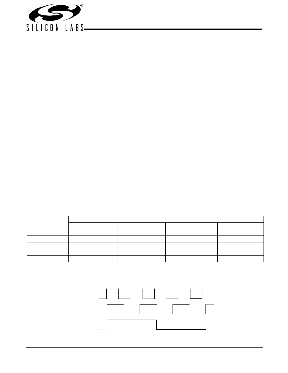
Table 1 shows the combinations of Pclk and Busclk
frequencies of greatest interest, organized by Gear Ratio.
Pclk
Synclk
Pclk/M =
Synclk/N
Figure 2. Gear Ratio Timing Diagram
Table 1. Supported Pclk and Busclk Frequencies, by Gear Ratio
Pclk
Gear Ratio and Busclk
2.0
1.5
1.33
1.0
67 MHz
267 MHz
100 MHz
300 MHz
400 MHz
133 MHz
267 MHz
356 MHz
400 MHz
150 MHz
400 MHz
200 MHz
400 MHz
相關(guān)PDF資料 |
PDF描述 |
|---|---|
| W158H | IC CLOCK CK98 SSCG CK98 56SSOP |
| W320-04H | IC CLK/DRVR CPUOUT 200MHZ 56SSOP |
| W681511S | IC VOICEBAND CODEC 5V 1CH 20SOP |
| X98014L128-3.3-Z | IC VIDEO DIGITIZER TRPL 128MQFP |
| X98017L128-3.3-Z | IC VIDEO DIGITIZER TRPL 128MQFP |
相關(guān)代理商/技術(shù)參數(shù) |
參數(shù)描述 |
|---|---|
| W134SSQC | 制造商:CYPRESS 制造商全稱:Cypress Semiconductor 功能描述:Direct Rambus Clock Generator |
| W134SSQCT | 制造商:CYPRESS 制造商全稱:Cypress Semiconductor 功能描述:Direct Rambus Clock Generator |
| W1351-015 | 制造商:MISCELLANEOUS 功能描述: 制造商: 功能描述: 制造商:undefined 功能描述: |
| W1352 | 制造商:Performance Tool 功能描述:45 Piece Power Bit Set 制造商:PERFORMANCE TOOLS 功能描述:45 PIECE POWER BIT SET |
| W135E11 | 制造商:OMRON INDUSTRIAL AUTOMATION 功能描述:Replaced by W135-E1-2B |
發(fā)布緊急采購,3分鐘左右您將得到回復(fù)。