- 您現(xiàn)在的位置:買賣IC網(wǎng) > PDF目錄359432 > VSC870TX (VITESSE SEMICONDUCTOR CORP) High Performance Serial Backplane Transceiver PDF資料下載
參數(shù)資料
| 型號(hào): | VSC870TX |
| 廠商: | VITESSE SEMICONDUCTOR CORP |
| 元件分類: | 通用總線功能 |
| 英文描述: | High Performance Serial Backplane Transceiver |
| 中文描述: | DUAL LINE TRANSCEIVER, PBGA192 |
| 封裝: | BGA-192 |
| 文件頁數(shù): | 36/40頁 |
| 文件大小: | 511K |
| 代理商: | VSC870TX |
第1頁第2頁第3頁第4頁第5頁第6頁第7頁第8頁第9頁第10頁第11頁第12頁第13頁第14頁第15頁第16頁第17頁第18頁第19頁第20頁第21頁第22頁第23頁第24頁第25頁第26頁第27頁第28頁第29頁第30頁第31頁第32頁第33頁第34頁第35頁當(dāng)前第36頁第37頁第38頁第39頁第40頁
VITESSE
Data Sheet
VSC870
High Performance Serial
Backplane Transceiver
Page 36
G52190-0, Rev 4.1
01/05/01
VITESSE
SEMICONDUCTOR CORPORATION
741 Calle Plano
Camarillo, CA 93012
Tel: (800) VITESSE
FAX: (805) 987-5896
Email: prodinfo@vitesse.com
Internet: www.vitesse.com
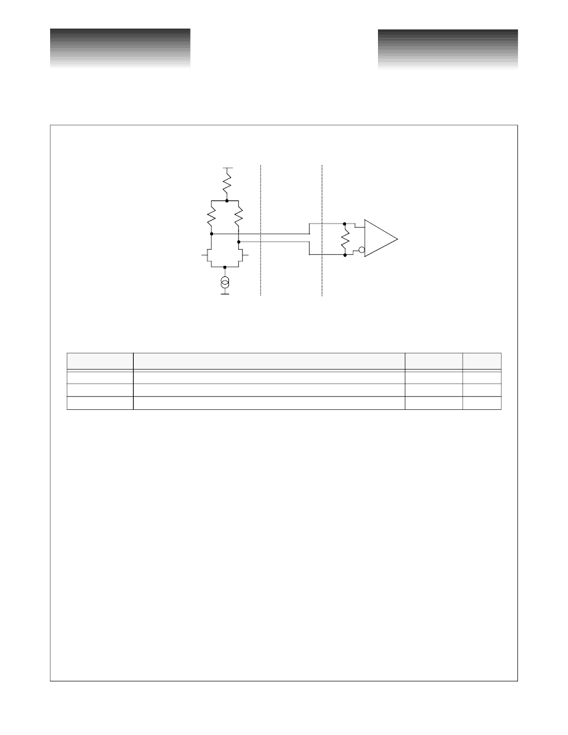
Figure 19: LVDS Input and Output Buffer Designs
Power Dissipation
Table 7: Power Supply Currents
Absolute Maximum Ratings
(1)
Power Supply Voltage (V
DD
) Potential to GND.................................................................................-0.5V to +4V
DC Input Voltage (LVDS inputs) ..........................................................................................-0.5V to V
DD
+ 1.0V
DC Input Voltage (TTL inputs).........................................................................................................-0.5V to 5.5V
DC Output Voltage (TTL outputs) ........................................................................................-0.5V to V
DD
+ 1.0V
Output Current (TTL outputs).................................................................................................................. +/-50mA
Output Current (LVDS outputs)................................................................................................................+/-50mA
Case Temperature Under Bias......................................................................................................-55
o
C to +125
o
C
Storage Temperature.....................................................................................................................-65
o
C to +150
o
C
NOTE: (1) Caution: Stresses listed under “Absolute Maximum Ratings” may be applied to devices one at a time without causing
permanent damage. Functionality at or exceeding the values listed is not implied. Exposure to these values for extended
periods may affect device reliability.
Recommended Operating Conditions
Power Supply Voltage (V
DD
, V
DDA
) ....................................................................................................+3.3V
Extended Commercial Operating Temperature Range
(1)
(T).............................................................. 0
o
C to 85
o
C
%
NOTE: (1) Lower limit of specification is ambient temperature and upper limit is case temperature.
Parameter
Description
(Max)
Units
I
DD
I
DDA
P
D
Power supply current from V
DD
and V
DDA
(V
DD
, V
DDA
= +3.3V + 5%)
Power supply current from V
DDA
(V
DDA
= +3.3V + 5%)
Power dissipation (V
DD
, V
DDA
= +3.3V + 5%)
1587
200
5.5
mA
mA
W
50
50
100
Receiver
Transmitter
Backplane
5
±
相關(guān)PDF資料 |
PDF描述 |
|---|---|
| VSC872 | 80 Gb/s Intelligent Switch Fabric |
| VSC874 | 10 Gbps Queue Manager with Integrated SPI4.2 Interface |
| VSC880 | High Performance 16x16 Serial Crosspoint Switch |
| VSC9110 | Target Specification |
| VSC9115 | 2.5 Gb/s Multi-Service SONET/SDH Mapper Device with Virtual Concatenation |
相關(guān)代理商/技術(shù)參數(shù) |
參數(shù)描述 |
|---|---|
| VSC872 | 制造商:VITESSE 制造商全稱:Vitesse Semiconductor Corporation 功能描述:80 Gb/s Intelligent Switch Fabric |
| VSC872TV01 | 制造商:Vitesse Semiconductor Corporation 功能描述: |
| VSC874 | 制造商:VITESSE 制造商全稱:Vitesse Semiconductor Corporation 功能描述:10 Gbps Queue Manager with Integrated SPI4.2 Interface |
| VSC880 | 制造商:VITESSE 制造商全稱:Vitesse Semiconductor Corporation 功能描述:High Performance 16x16 Serial Crosspoint Switch |
| VSC880TY | 制造商:VITESSE 制造商全稱:Vitesse Semiconductor Corporation 功能描述:High Performance 16x16 Serial Crosspoint Switch |
發(fā)布緊急采購,3分鐘左右您將得到回復(fù)。