- 您現(xiàn)在的位置:買賣IC網(wǎng) > PDF目錄359432 > VSC835 (Vitesse Semiconductor Corporation.) 34x34 Crosspoint Switch with Signal Detection PDF資料下載
參數(shù)資料
| 型號: | VSC835 |
| 廠商: | Vitesse Semiconductor Corporation. |
| 英文描述: | 34x34 Crosspoint Switch with Signal Detection |
| 中文描述: | 34x34交叉點開關(guān)信號檢測 |
| 文件頁數(shù): | 4/18頁 |
| 文件大?。?/td> | 174K |
| 代理商: | VSC835 |
VITESSE
Datasheet
VSC835
2.5 Gbits/sec
34x34 Crosspoint Switch with Signal Detection
Page 4
VITESSE
SEMICONDUCTOR CORPORATION
741 Calle Plano, Camarillo, CA 93012 805/388-3700 FAX: 805/987-5896
7/24/00
G52270-0, Rev. 4.1
If any change in a monitor state occurs after sampling by MONCLK, an interrupt will be signalled by
asserting INTB, and the user must identify the offending channel by reading the monitor states. The interrupt
will be cleared when the corresponding activity monitor is read, but the monitor state will not be changed. If
multiple monitors have triggered the interrupt, it will persist until all the corresponding monitors have been
read.
LOA requires a minimum signal level of 30-150mV peak-peak to recognize an input as active. This is
required to distinguish noise on an unconnected signal (where both inputs float to the termination voltage) from
activity on a live signal. A minimum of two transitions defines activity. The threshold signal level is controlled
by the voltage on the VHYS pin. In order to keep the hysteresis in a useful range, it is recommended that VHYS
be nominally tied to VCC (useful range is 2.0V to VCC ).
.
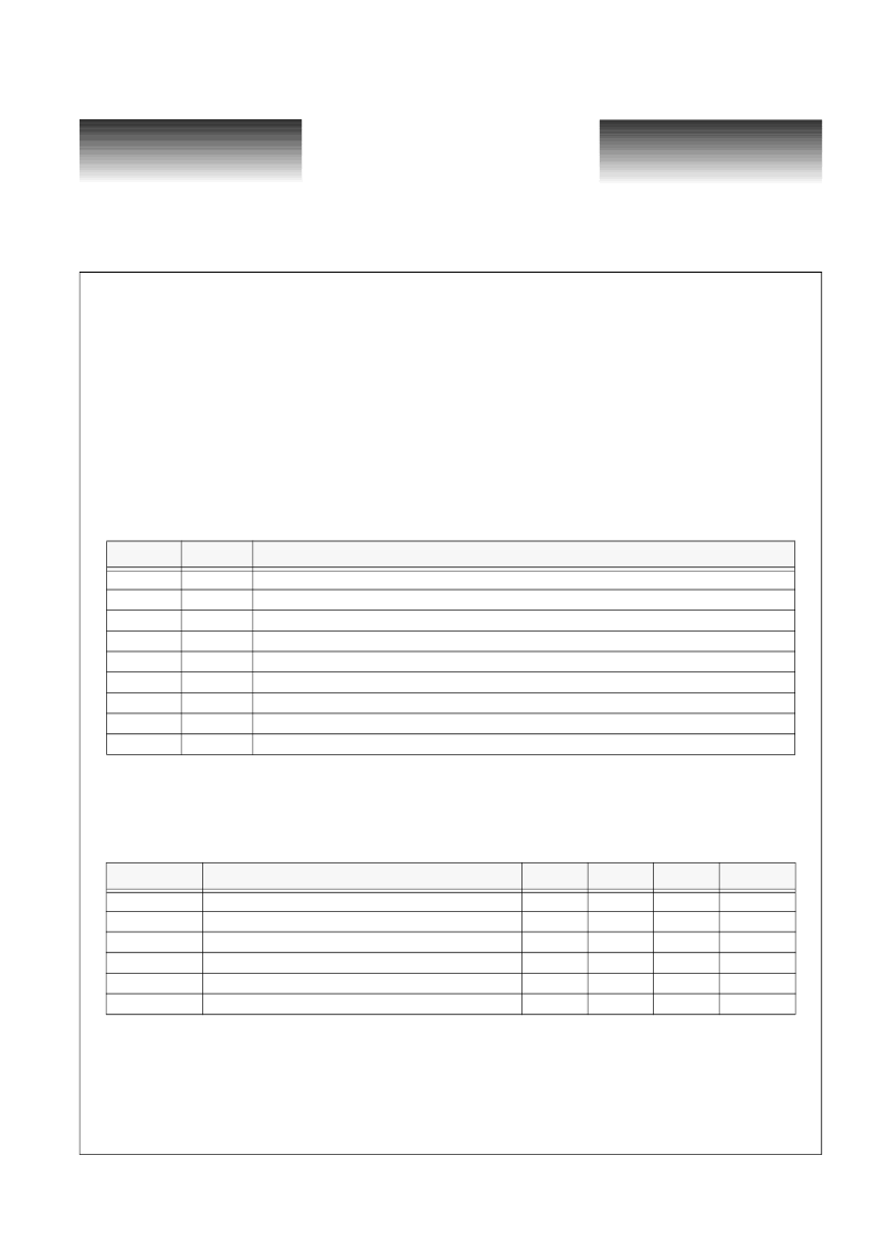
Table 2: Memory Map
AC Characteristics
note: Unless otherwise stated, all specifications are guaranteed but not tested.
note 1: Skew between any two input channels to a given output.
note 2: Skew between any two output channels from the same input channel.
note 3: Required for high-speed output rise/fall spec at F
RATE
=2.5 Gbits/s. For lower rate signals, use 0.375/F
RATE
note 4: Broadband jitter added to a jitter-free signal; jitter is primarily in the form of ISI for random data
Address
Access
Description
00h
01h
...
21h
R/W
R/W
...
R/W
R/O
R/O
R/O
R/O
R/O
Output Y0’s programmed input channel (write and then assert CONFIG to program)
Output Y1’s programmed input channel
...
Output Y33’s programmed input channel
Rx Signal monitor for inputs [A0-A3], [A4-A7] (Logic ‘1’=No activity)
Rx Signal monitor for inputs [A8-A11], [A12-A15]
Rx Signal monitor for inputs [A16-A19], [A20-A23]
Rx Signal monitor for inputs [A24-A27], [A28-A31]
Rx Signal monitor for inputs [A32-A33]
22h, 23h
24h, 25h
26h, 27h
28h, 29h
2Ah
Table 3: Data Path
Parameter
Description
Min
Typ
Max
Units
F
RATE
T
ISKW
T
OSKW
t
R
, t
F
t
R
, t
F
t
jP
Data rate
Input channel delay skew (1)
Output channel delay skew (2)
High-speed input rise/fall times, 20% to 80% (3)
High-speed output rise/fall times, 20% to 80%
Output data eye jitter, peak-peak, 2
31
PRBS (4)
-
-
-
-
-
-
-
2.5
-
-
150
150
100
Gbits/s
ps
ps
ps
ps
ps
300
300
-
-
-
相關(guān)PDF資料 |
PDF描述 |
|---|---|
| VSC837 | 3.2Gb/s 68x68 Crosspoint Switch |
| VSC837UG | DIODE ZENER SINGLE 150mW 3Vz 5mA-Izt 0.0667 10uA-Ir 1 SOT-523 3K/REEL |
| VSC838UG | RECTIFIER BRIDGE 25A 200V 300A-ifsm 1.1V-vf 5uA-ir GBPC 100/TRAY |
| VSC838 | 3.2Gb/s 36x37 Crosspoint Switch |
| VSC8476 | XAUI to XFI 10GE & 10GFC Transceiver |
相關(guān)代理商/技術(shù)參數(shù) |
參數(shù)描述 |
|---|---|
| VSC837 | 制造商:VITESSE 制造商全稱:Vitesse Semiconductor Corporation 功能描述:3.2Gb/s 68x68 Crosspoint Switch |
| VSC837UG | 制造商:Vitesse Semiconductor Corporation 功能描述: |
| VSC838 | 制造商:VITESSE 制造商全稱:Vitesse Semiconductor Corporation 功能描述:3.2Gb/s 36x37 Crosspoint Switch |
| VSC838UG | 制造商:VITESSE 制造商全稱:Vitesse Semiconductor Corporation 功能描述:3.2Gb/s 36x37 Crosspoint Switch |
| VSC8476 | 制造商:VITESSE 制造商全稱:Vitesse Semiconductor Corporation 功能描述:XAUI to XFI 10GE & 10GFC Transceiver |
發(fā)布緊急采購,3分鐘左右您將得到回復(fù)。