- 您現(xiàn)在的位置:買賣IC網(wǎng) > PDF目錄359432 > VSC838 (Vitesse Semiconductor Corporation.) 3.2Gb/s 36x37 Crosspoint Switch PDF資料下載
參數(shù)資料
| 型號: | VSC838 |
| 廠商: | Vitesse Semiconductor Corporation. |
| 英文描述: | 3.2Gb/s 36x37 Crosspoint Switch |
| 中文描述: | 達(dá)3.2GB / s的36x37交叉點(diǎn)開關(guān) |
| 文件頁數(shù): | 1/20頁 |
| 文件大小: | 296K |
| 代理商: | VSC838 |
VITESSE
Preliminary Data Sheet
VSC838
3.2Gb/s
36x37 Crosspoint Switch
G52351-0, Rev 3.0
02/12/01
Page 1
VITESSE
SEMICONDUCTOR CORPORATION
741 Calle Plano Camarillo, CA 93012
Tel: (800) VITESSE FAX: (805) 987-5896 Email: prodinfo@vitesse.com
Internet: www.vitesse.com
Features
36 Input by 37 Output Crosspoint Switch
3.2Gb/s NRZ Data Bandwidth
Non-Blocking Architecture Broadcast and Multicast
Capabilities
LVTTL/2.5V CMOS Control I/O (3.3V tolerant)
Input Signal Activity Monitoring Function
Integrated Signal Equalization (ISE) for Deterministic
Jitter Reduction
General Description
The VSC838 is a monolithic 36x36 asynchronous crosspoint switch, designed to carry broadband data
streams. The VSC838 also has an internal 37
th
output channel which is used in conjunction with the Activity
Monitor to allow in system diagnostics.
A high degree of signal integrity is maintained throughout the chip via fully differential signal paths.
The crosspoint function is based on a multiplexer array architecture. Each data output is driven by a 36:1
multiplexer that can be programmed to one and only one of its 36 inputs. The signal path is unregistered and
fully asynchronous, so there are not any restrictions on the phase, frequency, or signal pattern at each input.
Each high-speed output is a fully differential, switched current driver with switchable on-die terminations
for maximum signal integrity. Data inputs are terminated on-die through 100
impedance between true and
complement inputs (see
Input Termination
section for further details).
A dual mode programming interface is provided that allows programming commands to be sent as serial
data or parallel data. Core programming can be random for each port address, or multiple program assignments
can be queued and issued simultaneously. The programming may be initialized to a “straight-through” configu-
ration (A0 to Y0, A1 to Y1, etc.) using the INIT pin.
Unused channels may be powered down to allow efficient use of the switch in applications that require only
a subset of the channels. Power-down can be accomplished in hardware, via dedicated power pins for pairs of
input and output channels, or in software by programming individual unused outputs with a disable code.
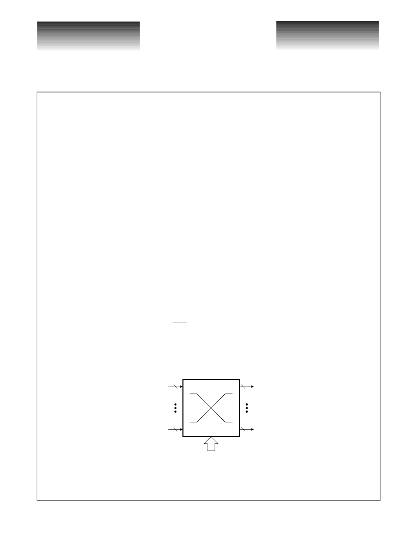
VSC838 Block Diagram
66MHz Dual Programming Port
Parallel and Serial programming modes
Programmable On-Chip I/O Termination
Differential CML Output Drivers
Single 2.5V Supply
6W Typical
—
Low Drive Mode
7W Typical
—
High Drive Mode
High Performance 37.5mm, 480 TBGA Package
2
2
2
2
A0
A35
Y0
Y35
μ
P
control
相關(guān)PDF資料 |
PDF描述 |
|---|---|
| VSC8476 | XAUI to XFI 10GE & 10GFC Transceiver |
| VSC8486 | 10 Gbps XAUI or XGMII to XFI LAN/WAN Transceiver |
| VSC850FX | Telecom Switching Circuit |
| VSC8558 | Octal Port 10/100/1000BASE-T and 1000BASE-X PHY |
| VSC8601 | 10/100/1000BASE-T PHY with RGMII and GMII MAC Interface |
相關(guān)代理商/技術(shù)參數(shù) |
參數(shù)描述 |
|---|---|
| VSC838UG | 制造商:VITESSE 制造商全稱:Vitesse Semiconductor Corporation 功能描述:3.2Gb/s 36x37 Crosspoint Switch |
| VSC8476 | 制造商:VITESSE 制造商全稱:Vitesse Semiconductor Corporation 功能描述:XAUI to XFI 10GE & 10GFC Transceiver |
| VSC8479 | 制造商:VITESSE 制造商全稱:Vitesse Semiconductor Corporation 功能描述:9.95 Gbps to 11.3 Gbps 16-bit Transceiver |
| VSC8479XYY | 制造商:Vitesse Semiconductor Corporation 功能描述:CHIPSET |
| VSC8486 | 制造商:VITESSE 制造商全稱:Vitesse Semiconductor Corporation 功能描述:10 Gbps XAUI or XGMII to XFI LAN/WAN Transceiver |
發(fā)布緊急采購,3分鐘左右您將得到回復(fù)。