- 您現(xiàn)在的位置:買(mǎi)賣(mài)IC網(wǎng) > PDF目錄200634 > UPC29S78 Useage of Three-Terminal Regulators | User's Manual[05/2000] PDF資料下載
參數(shù)資料
| 型號(hào): | UPC29S78 |
| 英文描述: | Useage of Three-Terminal Regulators | User's Manual[05/2000] |
| 中文描述: | 使用三端穩(wěn)壓器|用戶手冊(cè)[05/2000] |
| 文件頁(yè)數(shù): | 32/35頁(yè) |
| 文件大小: | 187K |
| 代理商: | UPC29S78 |
第1頁(yè)第2頁(yè)第3頁(yè)第4頁(yè)第5頁(yè)第6頁(yè)第7頁(yè)第8頁(yè)第9頁(yè)第10頁(yè)第11頁(yè)第12頁(yè)第13頁(yè)第14頁(yè)第15頁(yè)第16頁(yè)第17頁(yè)第18頁(yè)第19頁(yè)第20頁(yè)第21頁(yè)第22頁(yè)第23頁(yè)第24頁(yè)第25頁(yè)第26頁(yè)第27頁(yè)第28頁(yè)第29頁(yè)第30頁(yè)第31頁(yè)當(dāng)前第32頁(yè)第33頁(yè)第34頁(yè)第35頁(yè)
User’s Manual G12702EJ8V0UM00
6
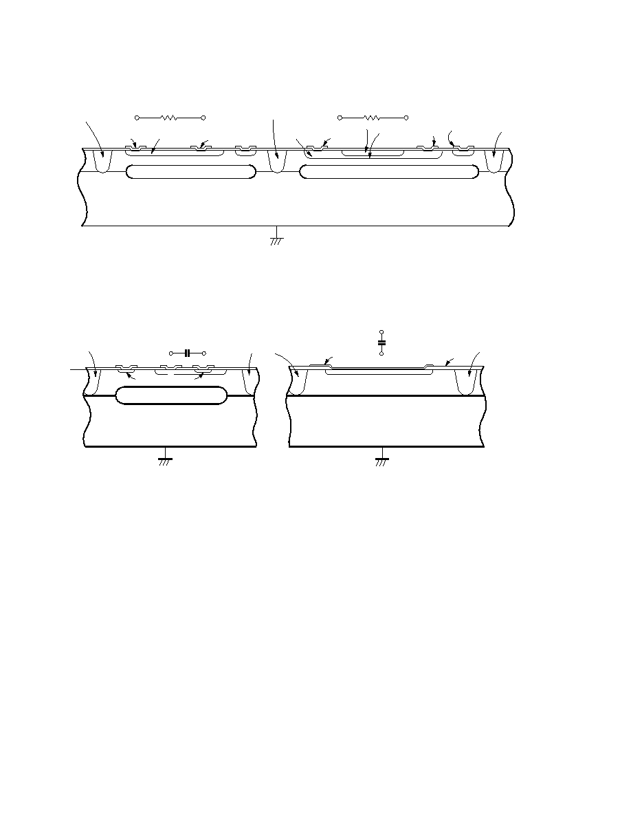
Figure 2-2. Structure of Resistor
Separation region
Base diffused resistor
Base pinch resistor
Pinch
region
Separation region
Separation
region
Epitaxial layer
electrode
Resistor
electrode
Resistor
electrode
Resistor
electrode
Resistor
electrode
P-type diffusion
layer
P-type diffusion
layer
P-type substrate
p
n+
n
n+ diffusion layer
Figure 2-3. Structure of Capacitor
Separation region
Junction capacitor
MOS capacitor
AI electrode
P-type substrate
n+
+
n
n+
p
pp
Oxide
layer
Separation region
n+
n
p
There is a point to heed in applying power supply ICs. It is that a method known as "junction separation" is used
as the method of electrically separating each of the elements above. By connecting a separation region so that it is
formed by a P-type semiconductor and is the same lowest potential as the substrate, the element region and the
separation region are electrically separated and insulated by being in (PN junction) reverse bias states. If for some
reason the potential of this separation region becomes a higher potential than the element region (for example the
NPN transistor collector region in Figure 2-1), normal operation cannot be expected since the PN junction enters a
forward bias state and the separation state between the elements cannot be maintained. For example, when using a
positive output three-terminal regulator, the GND pin always must be made a lower potential than the potential of
other pins.
2.2 About Power Supply IC Equivalent Circuits
Equivalent circuits that are shown in data sheets are so designated assuming the premise of the preceding
section (that separation regions and substrate are made the lowest potential). Be careful not to reference these
when this premise is violated.
相關(guān)PDF資料 |
PDF描述 |
|---|---|
| UPC3025 | Useage of Three-Terminal Regulators | User's Manual[05/2000] |
| UPC1663B | Analog IC |
| UPC1663C | Analog IC |
| UPC1663P | Analog IC |
| UPC1664C | Analog IC |
相關(guān)代理商/技術(shù)參數(shù) |
參數(shù)描述 |
|---|---|
| UPC29S78GR | 制造商:NEC 制造商全稱:NEC 功能描述:LOW DROPOUT VOLTAGE REGULATOR WITH ON/OFF FUNCTION |
| UPC29S78GR-E1-A | 制造商:Renesas Electronics Corporation 功能描述: |
| UPC29S78H | 制造商:NEC 制造商全稱:NEC 功能描述:LOW DROPOUT VOLTAGE REGULATOR WITH ON/OFF FUNCTION |
| UPC29S78TA | 制造商:NEC 制造商全稱:NEC 功能描述:LOW DROPOUT VOLTAGE REGULATOR WITH ON/OFF FUNCTION |
| UPC2A23P4 | 制造商: 功能描述: 制造商:undefined 功能描述: |
發(fā)布緊急采購(gòu),3分鐘左右您將得到回復(fù)。