- 您現(xiàn)在的位置:買賣IC網(wǎng) > PDF目錄1971 > TXS02326MRGER (Texas Instruments)IC SIM CARD MUX 2:1 24VQFN PDF資料下載
參數(shù)資料
| 型號(hào): | TXS02326MRGER |
| 廠商: | Texas Instruments |
| 文件頁數(shù): | 23/35頁 |
| 文件大小: | 0K |
| 描述: | IC SIM CARD MUX 2:1 24VQFN |
| 產(chǎn)品培訓(xùn)模塊: | Voltage Level Translation |
| 標(biāo)準(zhǔn)包裝: | 1 |
| 應(yīng)用: | 移動(dòng)電話 |
| 接口: | I²C |
| 電源電壓: | 1.7 V ~ 3.3 V |
| 封裝/外殼: | 24-VFQFN 裸露焊盤 |
| 供應(yīng)商設(shè)備封裝: | 24-VQFN 裸露焊盤(4x4) |
| 包裝: | 標(biāo)準(zhǔn)包裝 |
| 安裝類型: | 表面貼裝 |
| 其它名稱: | 296-28065-6 |
第1頁第2頁第3頁第4頁第5頁第6頁第7頁第8頁第9頁第10頁第11頁第12頁第13頁第14頁第15頁第16頁第17頁第18頁第19頁第20頁第21頁第22頁當(dāng)前第23頁第24頁第25頁第26頁第27頁第28頁第29頁第30頁第31頁第32頁第33頁第34頁第35頁
SCES795C
– SEPTEMBER 2010 – REVISED FEBRUARY 2011
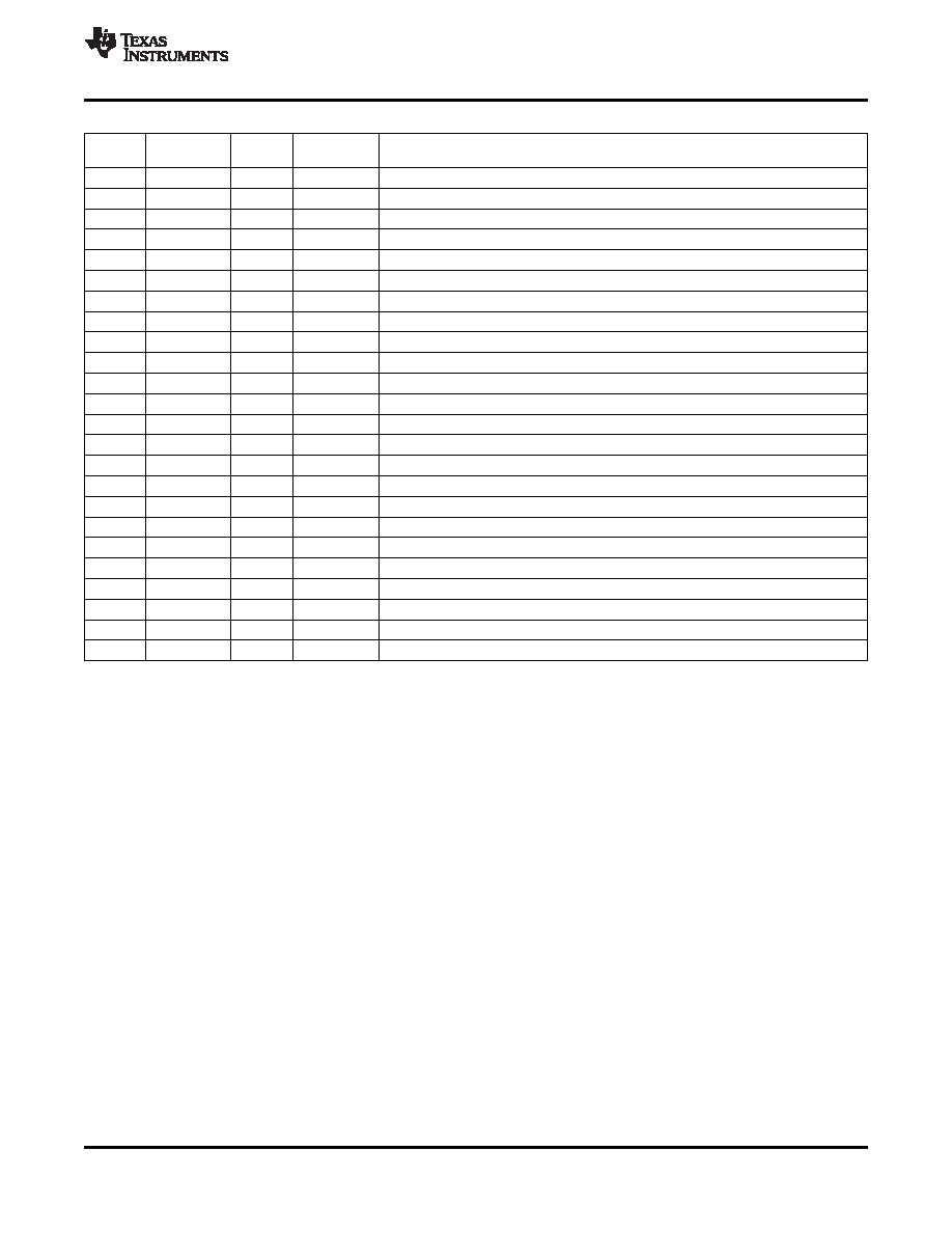
TERMINAL FUNCTIONS
POWER
NO.
NAME
TYPE(1)
DESCRIPTION
DOMAIN
1
IRQ
I/O
VDDIO
Interrupt to baseband. This signal is used to set the I2C address.
2
RSTX
I
VDDIO
Active-low reset input from baseband
3
SDN
I
VDDIO
Power down SIM2; for example, from switch
4
BSI
I
VDDIO
Analog signal from battery. This input accepts input voltages up to 3 V.
5
SIM2CLK
O
VSIM2
SIM2 clock
6
SIM2I/O
I/O
VSIM2
SIM2 data
7
SIM2RST
O
VSIM2
SIM2 reset
8
VSIM2
O
VSIM2
1.8 V/2.95 V supply voltage to SIM2
9
VBAT
P
VBAT
Battery power supply
10
GND
G
Ground
11
VSIM1
O
VSIM1
1.8 V/2.95 V supply voltage to SIM1
12
SIM1RST
O
VSIM1
SIM1 reset
13
SIM1I/O
I/O
VSIM1
SIM1 data
14
SIM1CLK
O
VSIM1
SIM1 clock
15
NC
No connect
16
SIMRST
I
VDDIO
UICC/SIM reset from baseband
17
SIMCLK
I
VDDIO
UICC/SIM clock
18
SIMI/O
I/O
VDDIO
UICC/SIM data
19
OE
I
VDDIO
UICC/SIM data direction from baseband
20
GND
G
21
VDDI/O
P
VDDIO
1.8-V power supply for device operation and I/O buffers toward baseband
22
CLK
I
VDDIO
32-kHz clock
23
SCK
I
VDDIO
I2C clock
24
SDA
I/O
VDDIO
I2C data
(1)
G = Ground, I = Input, O = Output, P = Power
2010–2011, Texas Instruments Incorporated
3
Product Folder Link(s): TXS02326
相關(guān)PDF資料 |
PDF描述 |
|---|---|
| TZA1026T/V2,118 | IC DATA AMPLIFIER 14-SOIC |
| TZA1038HW,118 | IC DVD SIGNAL PROC 48-HTQFP |
| UG80960HD5016SL2GM | IC MPU I960HD 3V 50MHZ 208-QFP |
| ULQ2003ATDG4Q1 | IC DARLINGTON TRANS ARRAY 16SOIC |
| UPD70F3025AGC-33-8EU-A | MCU 32BIT 256K FLASH 100LQFP |
相關(guān)代理商/技術(shù)參數(shù) |
參數(shù)描述 |
|---|---|
| TXS02326RGER | 功能描述:轉(zhuǎn)換 - 電壓電平 Dual-Supply Standby SIM Card Mux RoHS:否 制造商:Micrel 類型:CML/LVDS/LVPECL to LVCMOS/LVTTL 傳播延遲時(shí)間:1.9 ns 電源電流:14 mA 電源電壓-最大:3.6 V 電源電壓-最小:3 V 最大工作溫度:+ 85 C 安裝風(fēng)格:SMD/SMT 封裝 / 箱體:MLF-8 |
| TXS02612 | 制造商:TI 制造商全稱:Texas Instruments 功能描述:SDIO PORT EXANDER WITH VOLTAGE-LEVEL TRANSLATION |
| TXS02612_10 | 制造商:TI 制造商全稱:Texas Instruments 功能描述:SDIO PORT EXANDER WITH VOLTAGE-LEVEL TRANSLATION |
| TXS02612RTWR | 功能描述:轉(zhuǎn)換 - 電壓電平 SDIO Port Expander RoHS:否 制造商:Micrel 類型:CML/LVDS/LVPECL to LVCMOS/LVTTL 傳播延遲時(shí)間:1.9 ns 電源電流:14 mA 電源電壓-最大:3.6 V 電源電壓-最小:3 V 最大工作溫度:+ 85 C 安裝風(fēng)格:SMD/SMT 封裝 / 箱體:MLF-8 |
| TXS02612ZQSR | 功能描述:接口 - 專用 SDIO Port Expander RoHS:否 制造商:Texas Instruments 產(chǎn)品類型:1080p60 Image Sensor Receiver 工作電源電壓:1.8 V 電源電流:89 mA 最大功率耗散: 最大工作溫度:+ 85 C 安裝風(fēng)格:SMD/SMT 封裝 / 箱體:BGA-59 |
發(fā)布緊急采購,3分鐘左右您將得到回復(fù)。