- 您現(xiàn)在的位置:買賣IC網(wǎng) > PDF目錄383968 > TVP6000CPFP (Texas Instruments, Inc.) NTSC/PAL Digital Video Encoder PDF資料下載
參數(shù)資料
| 型號: | TVP6000CPFP |
| 廠商: | Texas Instruments, Inc. |
| 英文描述: | NTSC/PAL Digital Video Encoder |
| 中文描述: | NTSC / PAL數(shù)字視頻編碼器 |
| 文件頁數(shù): | 26/57頁 |
| 文件大小: | 268K |
| 代理商: | TVP6000CPFP |
第1頁第2頁第3頁第4頁第5頁第6頁第7頁第8頁第9頁第10頁第11頁第12頁第13頁第14頁第15頁第16頁第17頁第18頁第19頁第20頁第21頁第22頁第23頁第24頁第25頁當(dāng)前第26頁第27頁第28頁第29頁第30頁第31頁第32頁第33頁第34頁第35頁第36頁第37頁第38頁第39頁第40頁第41頁第42頁第43頁第44頁第45頁第46頁第47頁第48頁第49頁第50頁第51頁第52頁第53頁第54頁第55頁第56頁第57頁
2–14
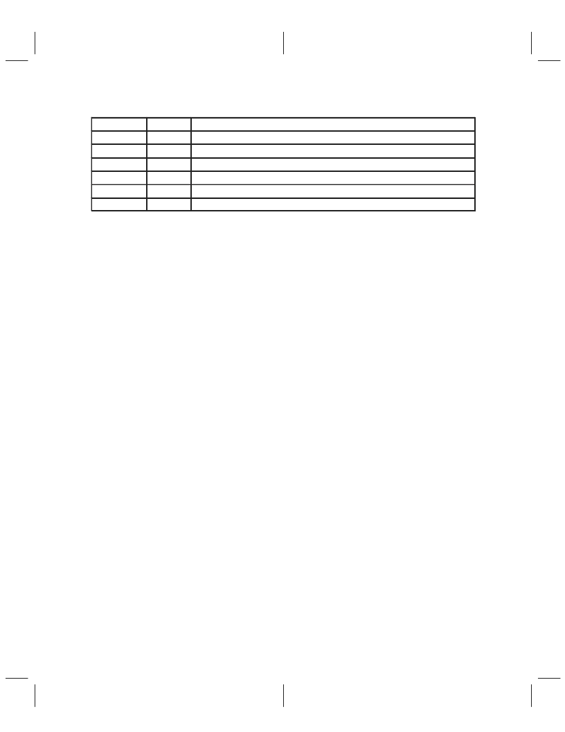
Table 2–6. Slave Mode Signals
PIN NAME
I/O TYPE
DESCRIPTION
LLC
Input
Line locked clock with 2X pixel clock frequency. CDIR pin is tied high.
Data phase reference clock. CDIR pin is tied high.
Output Vertical/Field timing, can be programmed as VSO/FSO/FSEQO
Can be programmed as VSI/FSI/FSEQI.
Programmed as CBNI.
Programmed as HSI.
CREF
Input
RCM1
Output
RCV1
Input
RCM2
Input
RCV2
Input
Refer to Table 2–15 and Table 2–17 for the definition of VSO, FSO, FSEQO, HSO, VSI, FSI, FSEQI, CBNI,
and HSI.
2.10.3
Demand mode is an interface specially designed for scan conversion. When scan conversion is enabled,
the TVP6000 accepts non-interlaced pixel data, performs signal processing functions which include
non-interlace-to-interlace conversion, flicker filtering and overscan-compensation, and outputs interlaced
NTSC/PAL video. Due to the nature of the functions that the TVP6000 performs during scan conversion,
the bandwidth of the input pixel increases and exceeds what the master and slave mode interface can
provide. Demand mode provides extra bandwidth to meet the needs of the TVP6000.
Demand Mode
Unlike master mode and slave mode, the video port interface timing for demand mode is decoupled from
the timing of the internal encoder core.
The TVP6000 operates in demand mode when it requests data from an external graphics controller or an
MPEG device. Demand mode is enabled by setting SCM[0] = 1, the SCN bit.
In demand mode, the TVP6000 asserts the RCM2 pin high to request additional data from the external
source and negates the RCM2 pin to stop additional data transfer. Table 2–19 shows how the RCM2 pin
may be programmed to operate as a request signal during demand mode. In addition, the NLR register is
used to program the threshold where the RCM2 pin is toggled for requests.
2.10.4
The TVP6000 may be configured in a genlock mode to an external TV decoder such as the
TVP5000/TVP5010 device. This configuration allows the decoder to drive video timing information to the
TVP6000 encoder. The genlock mode is used to control clock jitter and thus allows the encoder to generate
accurate color burst information.
Genlock Mode
In this configuration, GLCI pin is connected to the GLCO pin of the decoder, and the line-lock clock pin, LLC,
is fed by the decoder main pixel clock output. Moreover, the color sub-carrier information is formatted as
a 23-bit binary number and is transmitted serially. The transmission timing diagram is shown in Figure 2–13.
相關(guān)PDF資料 |
PDF描述 |
|---|---|
| TVS0603SMD | VARISTORS (Multilayer Ceramic Transient Voltage Suppressor Standard Capacity) |
| TVS0805SMD | VARISTORS (Multilayer Ceramic Transient Voltage Suppressor Standard Capacity) |
| TVS1206SMD | 2.0mV Quad Micropower Rail-to-Rail CMOS Operational Amplifier, 14L CDIP |
| TX02-4400 | Interface Transformer |
| U1160 | small Photocell Glass encapsulated housing |
相關(guān)代理商/技術(shù)參數(shù) |
參數(shù)描述 |
|---|---|
| TVP7000 | 制造商:Texas Instruments 功能描述:Triple 8-bit Digitizer 150MSPS TVP7000 |
| TVP7000EVM | 功能描述:視頻 IC 開發(fā)工具 TVP7000 Eval Mod RoHS:否 制造商:Texas Instruments 產(chǎn)品:Evaluation Boards 類型:YPbPr to RGBHV Converters 工具用于評估:LMH1251 工作電源電壓:5 V |
| TVP7000PZP | 功能描述:視頻模擬/數(shù)字化轉(zhuǎn)換器集成電路 Triple 8/10B 150/110 MSPS Video ADC RoHS:否 制造商:Texas Instruments 輸入信號類型:Differential 轉(zhuǎn)換器數(shù)量:1 ADC 輸入端數(shù)量:4 轉(zhuǎn)換速率:3 Gbps 分辨率:8 bit 結(jié)構(gòu): 輸入電壓:3.3 V 接口類型:SPI 信噪比: 電壓參考: 電源電壓-最大:3.45 V 電源電壓-最小:3.15 V 最大功率耗散: 最大工作溫度:+ 85 C 最小工作溫度:- 40 C 封裝 / 箱體:TCSP-48 封裝:Reel |
| TVP7000PZPR | 功能描述:視頻模擬/數(shù)字化轉(zhuǎn)換器集成電路 Tr 8/10B 150/110 MSPS Video ADC RoHS:否 制造商:Texas Instruments 輸入信號類型:Differential 轉(zhuǎn)換器數(shù)量:1 ADC 輸入端數(shù)量:4 轉(zhuǎn)換速率:3 Gbps 分辨率:8 bit 結(jié)構(gòu): 輸入電壓:3.3 V 接口類型:SPI 信噪比: 電壓參考: 電源電壓-最大:3.45 V 電源電壓-最小:3.15 V 最大功率耗散: 最大工作溫度:+ 85 C 最小工作溫度:- 40 C 封裝 / 箱體:TCSP-48 封裝:Reel |
| TVP7001 | 制造商:Texas Instruments 功能描述:Triple 8-bit Digitizer 165MSPS TVP7001 |
發(fā)布緊急采購,3分鐘左右您將得到回復(fù)。