- 您現(xiàn)在的位置:買賣IC網(wǎng) > PDF目錄383960 > TMX32C6411AGLZ (Texas Instruments, Inc.) FIXED POINT DIGITAL SIGNAL PROCESSOR PDF資料下載
參數(shù)資料
| 型號: | TMX32C6411AGLZ |
| 廠商: | Texas Instruments, Inc. |
| 元件分類: | 數(shù)字信號處理 |
| 英文描述: | FIXED POINT DIGITAL SIGNAL PROCESSOR |
| 中文描述: | 定點(diǎn)數(shù)字信號處理器 |
| 文件頁數(shù): | 69/119頁 |
| 文件大?。?/td> | 1742K |
| 代理商: | TMX32C6411AGLZ |
第1頁第2頁第3頁第4頁第5頁第6頁第7頁第8頁第9頁第10頁第11頁第12頁第13頁第14頁第15頁第16頁第17頁第18頁第19頁第20頁第21頁第22頁第23頁第24頁第25頁第26頁第27頁第28頁第29頁第30頁第31頁第32頁第33頁第34頁第35頁第36頁第37頁第38頁第39頁第40頁第41頁第42頁第43頁第44頁第45頁第46頁第47頁第48頁第49頁第50頁第51頁第52頁第53頁第54頁第55頁第56頁第57頁第58頁第59頁第60頁第61頁第62頁第63頁第64頁第65頁第66頁第67頁第68頁當(dāng)前第69頁第70頁第71頁第72頁第73頁第74頁第75頁第76頁第77頁第78頁第79頁第80頁第81頁第82頁第83頁第84頁第85頁第86頁第87頁第88頁第89頁第90頁第91頁第92頁第93頁第94頁第95頁第96頁第97頁第98頁第99頁第100頁第101頁第102頁第103頁第104頁第105頁第106頁第107頁第108頁第109頁第110頁第111頁第112頁第113頁第114頁第115頁第116頁第117頁第118頁第119頁
SPRS196H MARCH 2002 REVISED JULY 2004
69
POST OFFICE BOX 1443
HOUSTON, TEXAS 772511443
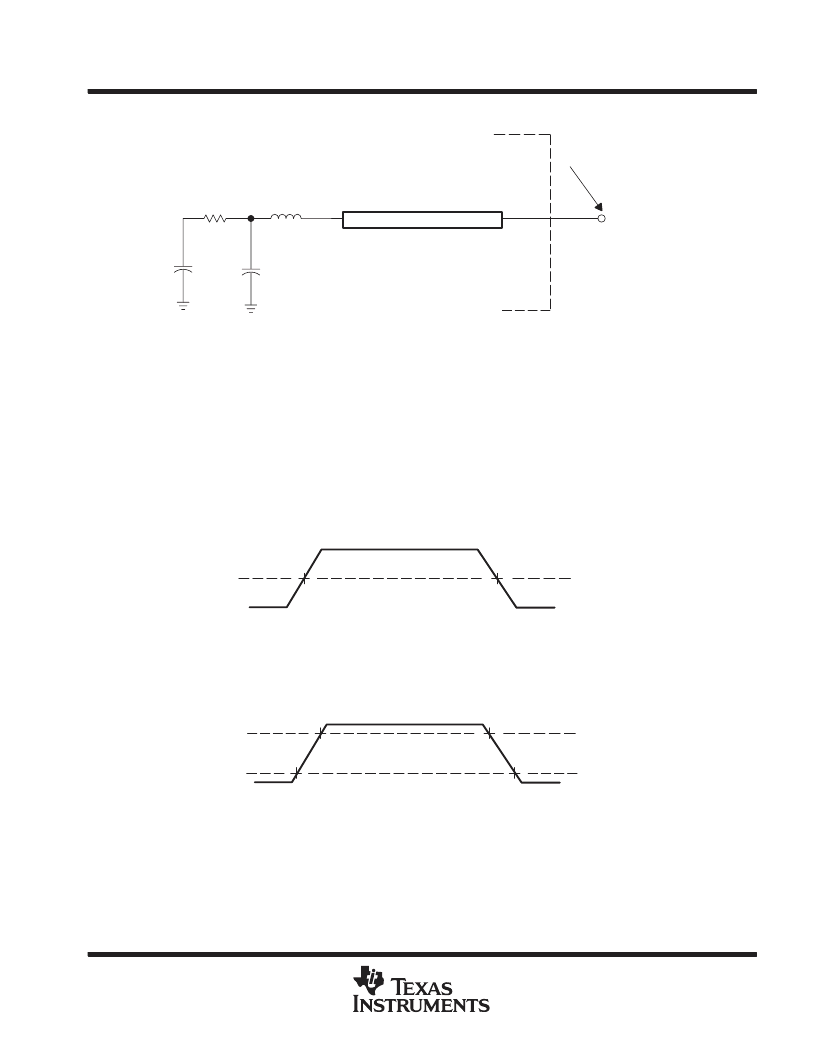
PARAMETER MEASUREMENT INFORMATION
Transmission Line
4.0 pF
1.85 pF
Z0 = 50
(see note)
Tester Pin Electronics
Data Sheet Timing Reference Point
Output
Under
Test
NOTE: The data sheet provides timing at the device pin. For output timing analysis, the tester pin electronics and its transmission line effects
must be taken into account. A transmission line with a delay of 2 ns or longer can be used to produce the desired transmission line effect.
The transmission line is intended as a load only. It is not necessary to add or subtract the transmission line delay (2 ns or longer) from
the data sheet timings.
Input requirements in this data sheet are tested with an input slew rate of < 4 Volts per nanosecond (4 V/ns) at the device pin.
42
3.5 nH
Device Pin
(see note)
Figure 12. Test Load Circuit for AC Timing Measurements
The tester load circuit is for characterization and measurement of AC timing signals. This load does not indicate
the maximum load the device is capable of driving.
signal transition levels
All input and output timing parameters are referenced to 1.5 V for both “0” and “1” logic levels.
Vref = 1.5 V
Figure 13. Input and Output Voltage Reference Levels for AC Timing Measurements
All rise and fall transition timing parameters are referenced to V
IL
MAX and V
IH
MIN for input clocks, V
OL
MAX
and V
OH
MIN for output clocks, V
ILP
MAX and V
IHP
MIN for PCI input clocks, and V
OLP
MAX and V
OHP
MIN for
PCI output clocks.
Vref = VIL MAX (or VOL MAX or
VILP MAX or VOLP MAX)
Vref = VIH MIN (or VOH MIN or
VIHP MIN or VOHP MIN)
Figure 14. Rise and Fall Transition Time Voltage Reference Levels
signal transition rates
All timings are tested with an input edge rate of 4 Volts per nanosecond (4 V/ns).
相關(guān)PDF資料 |
PDF描述 |
|---|---|
| TMP32C6411AZLZ | FIXED POINT DIGITAL SIGNAL PROCESSOR |
| TMP320C6411AZLZ | FIXED POINT DIGITAL SIGNAL PROCESSOR |
| TMX32C6411AZLZ | ER 5C 2#6 3#4 SKT PLUG |
| TMP320C6411ZLZ | FIXED POINT DIGITAL SIGNAL PROCESSOR |
| TMX32C6411ZLZ | FIXED POINT DIGITAL SIGNAL PROCESSOR |
相關(guān)代理商/技術(shù)參數(shù) |
參數(shù)描述 |
|---|---|
| TMX32C6414EGLZ6E3 | 制造商:Rochester Electronics LLC 功能描述:- Bulk |
| TMX32C6415EGLZ5E0 | 制造商:Rochester Electronics LLC 功能描述:LAPLACE, REV. 2.0, 500 MHZ, 100 MHZ EMIF - Bulk |
| TMX32C6416EGLZ5E0 | 制造商:Rochester Electronics LLC 功能描述:- Bulk |
| TMX32TCI6482BZTZA2 | 制造商:Texas Instruments 功能描述: |
| TMX32TCI6616BXCYPA | 制造商:Texas Instruments 功能描述: |
發(fā)布緊急采購,3分鐘左右您將得到回復(fù)。