- 您現(xiàn)在的位置:買賣IC網(wǎng) > PDF目錄383960 > TMX320C6411AZLZ (Texas Instruments, Inc.) FIXED POINT DIGITAL SIGNAL PROCESSOR PDF資料下載
參數(shù)資料
| 型號: | TMX320C6411AZLZ |
| 廠商: | Texas Instruments, Inc. |
| 元件分類: | 數(shù)字信號處理 |
| 英文描述: | FIXED POINT DIGITAL SIGNAL PROCESSOR |
| 中文描述: | 定點數(shù)字信號處理器 |
| 文件頁數(shù): | 68/119頁 |
| 文件大小: | 1742K |
| 代理商: | TMX320C6411AZLZ |
第1頁第2頁第3頁第4頁第5頁第6頁第7頁第8頁第9頁第10頁第11頁第12頁第13頁第14頁第15頁第16頁第17頁第18頁第19頁第20頁第21頁第22頁第23頁第24頁第25頁第26頁第27頁第28頁第29頁第30頁第31頁第32頁第33頁第34頁第35頁第36頁第37頁第38頁第39頁第40頁第41頁第42頁第43頁第44頁第45頁第46頁第47頁第48頁第49頁第50頁第51頁第52頁第53頁第54頁第55頁第56頁第57頁第58頁第59頁第60頁第61頁第62頁第63頁第64頁第65頁第66頁第67頁當(dāng)前第68頁第69頁第70頁第71頁第72頁第73頁第74頁第75頁第76頁第77頁第78頁第79頁第80頁第81頁第82頁第83頁第84頁第85頁第86頁第87頁第88頁第89頁第90頁第91頁第92頁第93頁第94頁第95頁第96頁第97頁第98頁第99頁第100頁第101頁第102頁第103頁第104頁第105頁第106頁第107頁第108頁第109頁第110頁第111頁第112頁第113頁第114頁第115頁第116頁第117頁第118頁第119頁
SPRS196H MARCH 2002 REVISED JULY 2004
68
POST OFFICE BOX 1443
HOUSTON, TEXAS 772511443
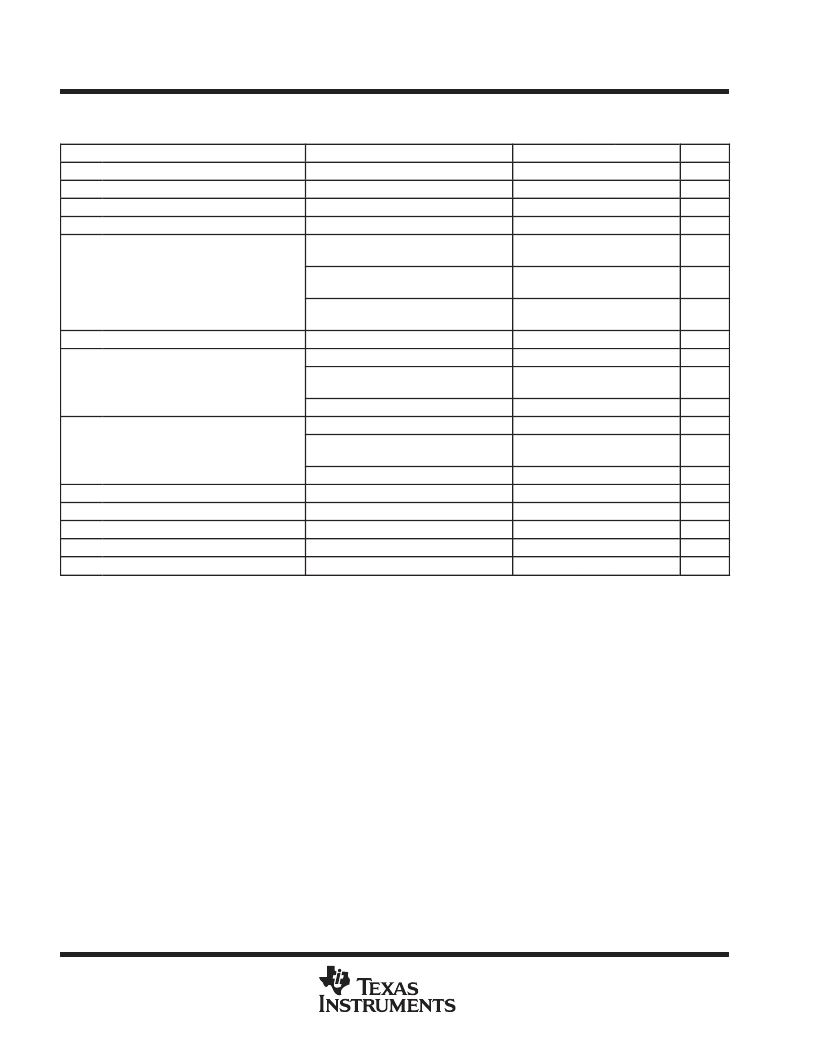
electrical characteristics over recommended ranges of supply voltage and operating case
temperature (unless otherwise noted)
PARAMETER
TEST CONDITIONS
DVDD
= MIN,
IOHP = 0.5 mA,
DVDD
= MIN,
IOLP = 1.5 mA,
VI
= VSS to DVDD no opposing internal
resistor
VI
= VSS to DVDD opposing internal
pullup resistor
VI
= VSS to DVDD opposing internal
pulldown resistor
0 < VIP
< DVDD,
EMIF, CLKOUT4, CLKOUT6, EMUx
MIN
TYP
MAX
UNIT
VOH
VOHP
VOL
VOLP
High-level output voltage (except PCI)
IOH = MAX
DVDD = 3.3 V
IOL = MAX
DVDD = 3.3 V
2.4
V
High-level output voltage (PCI)
0.9DVDD
V
Low-level output voltage (except PCI)
0.4
V
Low-level output voltage (PCI)
0.1DVDD
V
±
10
uA
II
Input current (except PCI)
50
100
150
uA
150
100
50
uA
IIP
Input leakage current (PCI)§
DVDD = 3.3 V
±
10
16
uA
mA
IOH
High-level output current
Timer, TDO, GPIO
(Excluding GP[15:9, 2, 1]), McBSP
8
mA
PCI/HPI
0.5§
mA
EMIF, CLKOUT4, CLKOUT6, EMUx
16
mA
IOL
Low-level output current
Timer, TDO, GPIO
(Excluding GP[15:9, 2, 1]), McBSP
8
mA
PCI/HPI
VO
= DVDD or 0 V
CVDD
= 1.2 V, CPU clock = 300 MHz
DVDD
= 3.3 V, CPU clock = 300 MHz
1.5
mA
IOZ
ICDD
IDDD
Ci
Co
For test conditions shown as MIN, MAX, or NOM, use the appropriate value specified in the recommended operating conditions table.
Applies only to pins with an internal pullup (IPU) or pulldown (IPD) resistor.
§PCI input leakage currents include Hi-Z output leakage for all bidirectional buffers with 3-state outputs.
These rated numbers are from the PCI specification version 2.3. The DC specification and AC specification are defined in Tables 4-3 and 4-4,
respectively.
#Measured with average activity (50% high/50% low power). The actual current draw is highly application-dependent. For more details on core
and I/O activity, refer to the
TMS320C6411 Power Consumption Summary
application report (literature number SPRA373).
Off-state output current
Core supply current#
I/O supply current#
±
10
uA
550
mA
125
mA
Input capacitance
10
pF
Output capacitance
10
pF
recommended clock and control signal transition behavior
All clocks and control signals
must
transition between V
IH
and V
IL
(or between V
IL
and V
IH
) in a monotonic
manner.
相關(guān)PDF資料 |
PDF描述 |
|---|---|
| TMX320C6411GLZ | FIXED POINT DIGITAL SIGNAL PROCESSOR |
| TMX320C6411ZLZ | FIXED POINT DIGITAL SIGNAL PROCESSOR |
| TMX32C6411AGLZ | FIXED POINT DIGITAL SIGNAL PROCESSOR |
| TMP32C6411AZLZ | FIXED POINT DIGITAL SIGNAL PROCESSOR |
| TMP320C6411AZLZ | FIXED POINT DIGITAL SIGNAL PROCESSOR |
相關(guān)代理商/技術(shù)參數(shù) |
參數(shù)描述 |
|---|---|
| TMX320C6411GLZ | 制造商:Rochester Electronics LLC 功能描述:C6411 1V/300MHZ PROTOTYPES - Bulk 制造商:Texas Instruments 功能描述: |
| TMX320C6411GLZ300 | 制造商:TI 制造商全稱:Texas Instruments 功能描述:FIXED-POINT DIGITAL SIGNAL PROCESSORS |
| TMX320C6411GLZ5E0 | 制造商:TI 制造商全稱:Texas Instruments 功能描述:FIXED-POINT DIGITAL SIGNAL PROCESSORS |
| TMX320C6411GLZA300 | 制造商:TI 制造商全稱:Texas Instruments 功能描述:FIXED-POINT DIGITAL SIGNAL PROCESSORS |
| TMX320C6411GLZA5E0 | 制造商:TI 制造商全稱:Texas Instruments 功能描述:FIXED-POINT DIGITAL SIGNAL PROCESSORS |
發(fā)布緊急采購,3分鐘左右您將得到回復(fù)。