- 您現在的位置:買賣IC網 > PDF目錄382635 > TMS320F241PGQ 16-Bit Digital Signal Processor PDF資料下載
參數資料
| 型號: | TMS320F241PGQ |
| 元件分類: | 數字信號處理 |
| 英文描述: | 16-Bit Digital Signal Processor |
| 中文描述: | 16位數字信號處理器 |
| 文件頁數: | 8/116頁 |
| 文件大小: | 1485K |
| 代理商: | TMS320F241PGQ |
第1頁第2頁第3頁第4頁第5頁第6頁第7頁當前第8頁第9頁第10頁第11頁第12頁第13頁第14頁第15頁第16頁第17頁第18頁第19頁第20頁第21頁第22頁第23頁第24頁第25頁第26頁第27頁第28頁第29頁第30頁第31頁第32頁第33頁第34頁第35頁第36頁第37頁第38頁第39頁第40頁第41頁第42頁第43頁第44頁第45頁第46頁第47頁第48頁第49頁第50頁第51頁第52頁第53頁第54頁第55頁第56頁第57頁第58頁第59頁第60頁第61頁第62頁第63頁第64頁第65頁第66頁第67頁第68頁第69頁第70頁第71頁第72頁第73頁第74頁第75頁第76頁第77頁第78頁第79頁第80頁第81頁第82頁第83頁第84頁第85頁第86頁第87頁第88頁第89頁第90頁第91頁第92頁第93頁第94頁第95頁第96頁第97頁第98頁第99頁第100頁第101頁第102頁第103頁第104頁第105頁第106頁第107頁第108頁第109頁第110頁第111頁第112頁第113頁第114頁第115頁第116頁
TMS320F243, TMS320F241
DSP CONTROLLERS
SPRS064B – DECEMBER 1997 – REVISED FEBRUARY 1999
8
POST OFFICE BOX 1443
HOUSTON, TEXAS 77251–1443
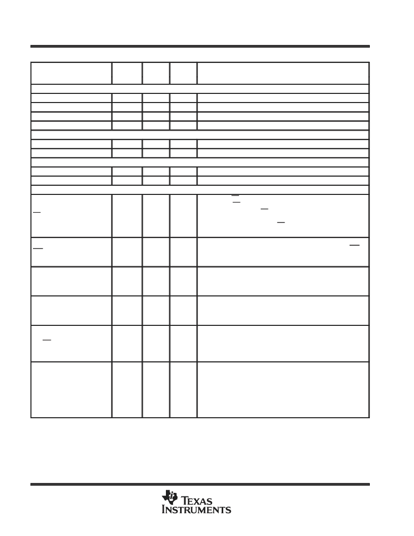
Terminal Functions - ’F243 PGE Package (Continued)
NAME
144
QFP
NO.
TYPE
RESET
STATE
DESCRIPTION
SERIAL PERIPHERAL INTERFACE (SPI) AND BIT I/O PINS
SPISIMO/
IOPC2
60
I/O
I
SPI slave in, master out or GPIO
SPISOMI/
IOPC3
62
I/O
I
SPI slave out, master in or GPIO
SPICLK/
IOPC4
64
I/O
I
SPI clock or GPIO
SPISTE/
IOPC5
66
I/O
I
SPI slave transmit enable (optional) or GPIO
SERIAL COMMUNICATIONS INTERFACE (SCI) AND BIT I/O PINS
SCITXD/
IOPA0
56
I/O
I
SCI asynchronous serial port transmit data or GPIO
SCIRXD/
IOPA1
58
I/O
I
SCI asynchronous serial port receive data or GPIO
CONTROLLER AREA NETWORK (CAN)
CANTX/
IOPC6
115
I/O
I
CAN transmit data or GPIO
CANRX/
IOPC7
113
I/O
I
CAN receive data or GPIO
INTERRUPT, EXTERNAL ACCESS, AND MISCELLANEOUS SIGNALS
RS
19
I/O
I
Device reset. RS causes the ’F243/241 to terminate execution and sets
PC = 0. When RS is brought to a high level, execution begins at location
zero of program memory. RS affects (or sets to zero) various registers
and status bits. When the watchdog timer overflows, it initiates a system
reset pulse that is reflected on the RS pin. This pulse is eight clock cycles
wide.
NMI§
79
I
I
Nonmaskable interrupt. When NMI is activated, the device is interrupted
regardless of the state of the INTM bit of the status register. NMI is
(falling) edge- and low-level-sensitive. To be recognized by the core, this
pin must be kept low for at least one clock cycle after the falling edge.
XINT1/
IOPA2
83
I/O
I
External user interrupt 1 or GPIO. Both XINT1 and XINT2 are edge-
sensitive. To be recognized by the core, these pins must be kept
high/low for at least one clock cycle after the edge. The edge polarity is
programmable.
XINT2/ADCSOC/
IOPD1
81
I/O
I
External user interrupt 2. External “start-of-conversion” input for
ADC/GPIO. Both XINT1 and XINT2 are edge-sensitive. To be
recognized by the core, these pins must be kept high/low for at least one
clock cycle after the edge. The edge polarity is programmable.
MP/MC
43
I
I
Microprocessor/Microcomputer mode select. If this pin is low during
reset, the device is put in microcomputer mode and program execution
begins at 0000h of internal program memory (flash EEPROM). A high
value during reset puts the device in microprocessor mode and program
execution begins at 0000h of external program memory.
READY
44
I
I
READY is pulled low to add wait states for external accesses. READY
indicates that an external device is prepared for a bus transaction to be
completed. If the device is not ready, it pulls the READY pin low. The
processor waits one cycle and checks READY again. Note that the
processor performs READY-detection if at least one software wait state
is programmed. To meet the external READY timings, the wait-state
generator control register (WSGR) should be programmed for at least
one wait state.
I = input, O = output, Z = high impedance
The reset state indicates the state of the pin at reset. If the pin is an input, indicated by an I, its state is determined by user design. If the pin is
an output, its level at reset is indicated.
§ In silicon revisions 2.0-TMX and 2.1-TMS, this pin is level-sensitive and can cause multiple interrupts when held low.
Data is in output mode when AVIS is enabled. At reset, the device comes up with AVIS mode enabled. The data bus is in output mode while AVIS
is enabled.
NOTE:
Bold, italicized pin names
indicate pin function after reset.
相關PDF資料 |
PDF描述 |
|---|---|
| TMS320F243PGEQ | 16-Bit Digital Signal Processor |
| TMS320F243PGES | 16-Bit Digital Signal Processor |
| TMS320C3X | 32-Bit Digital Signal Processor |
| TMS320C4X | Digital Signal Processing Solutions |
| TMS320C6454GTZ7 | Fixed-Point Digital Signal Processor |
相關代理商/技術參數 |
參數描述 |
|---|---|
| TMS320F241PGS | 功能描述:數字信號處理器和控制器 - DSP, DSC 16B 5V fixed point DSP w/ Flash RoHS:否 制造商:Microchip Technology 核心:dsPIC 數據總線寬度:16 bit 程序存儲器大小:16 KB 數據 RAM 大小:2 KB 最大時鐘頻率:40 MHz 可編程輸入/輸出端數量:35 定時器數量:3 設備每秒兆指令數:50 MIPs 工作電源電壓:3.3 V 最大工作溫度:+ 85 C 封裝 / 箱體:TQFP-44 安裝風格:SMD/SMT |
| TMS320F243PGE | 功能描述:數字信號處理器和控制器 - DSP, DSC 16B 5V fixed point DSP w/ Flash RoHS:否 制造商:Microchip Technology 核心:dsPIC 數據總線寬度:16 bit 程序存儲器大小:16 KB 數據 RAM 大小:2 KB 最大時鐘頻率:40 MHz 可編程輸入/輸出端數量:35 定時器數量:3 設備每秒兆指令數:50 MIPs 工作電源電壓:3.3 V 最大工作溫度:+ 85 C 封裝 / 箱體:TQFP-44 安裝風格:SMD/SMT |
| TMS320F243PGEA | 功能描述:數字信號處理器和控制器 - DSP, DSC 16B 5V fixed point DSP w/ Flash RoHS:否 制造商:Microchip Technology 核心:dsPIC 數據總線寬度:16 bit 程序存儲器大小:16 KB 數據 RAM 大小:2 KB 最大時鐘頻率:40 MHz 可編程輸入/輸出端數量:35 定時器數量:3 設備每秒兆指令數:50 MIPs 工作電源電壓:3.3 V 最大工作溫度:+ 85 C 封裝 / 箱體:TQFP-44 安裝風格:SMD/SMT |
| TMS320F28015PZA | 功能描述:數字信號處理器和控制器 - DSP, DSC 32-Bit DSC w/ 32KB Flash RoHS:否 制造商:Microchip Technology 核心:dsPIC 數據總線寬度:16 bit 程序存儲器大小:16 KB 數據 RAM 大小:2 KB 最大時鐘頻率:40 MHz 可編程輸入/輸出端數量:35 定時器數量:3 設備每秒兆指令數:50 MIPs 工作電源電壓:3.3 V 最大工作溫度:+ 85 C 封裝 / 箱體:TQFP-44 安裝風格:SMD/SMT |
| TMS320F28015PZA | 制造商:Texas Instruments 功能描述:IC DSP 32-BIT CMOS QFP 100PIN PLAS |
發(fā)布緊急采購,3分鐘左右您將得到回復。