- 您現(xiàn)在的位置:買賣IC網(wǎng) > PDF目錄383960 > TMP32C6411ZLZ (Texas Instruments, Inc.) FIXED POINT DIGITAL SIGNAL PROCESSOR PDF資料下載
參數(shù)資料
| 型號: | TMP32C6411ZLZ |
| 廠商: | Texas Instruments, Inc. |
| 元件分類: | 數(shù)字信號處理 |
| 英文描述: | FIXED POINT DIGITAL SIGNAL PROCESSOR |
| 中文描述: | 定點數(shù)字信號處理器 |
| 文件頁數(shù): | 41/119頁 |
| 文件大?。?/td> | 1742K |
| 代理商: | TMP32C6411ZLZ |
第1頁第2頁第3頁第4頁第5頁第6頁第7頁第8頁第9頁第10頁第11頁第12頁第13頁第14頁第15頁第16頁第17頁第18頁第19頁第20頁第21頁第22頁第23頁第24頁第25頁第26頁第27頁第28頁第29頁第30頁第31頁第32頁第33頁第34頁第35頁第36頁第37頁第38頁第39頁第40頁當前第41頁第42頁第43頁第44頁第45頁第46頁第47頁第48頁第49頁第50頁第51頁第52頁第53頁第54頁第55頁第56頁第57頁第58頁第59頁第60頁第61頁第62頁第63頁第64頁第65頁第66頁第67頁第68頁第69頁第70頁第71頁第72頁第73頁第74頁第75頁第76頁第77頁第78頁第79頁第80頁第81頁第82頁第83頁第84頁第85頁第86頁第87頁第88頁第89頁第90頁第91頁第92頁第93頁第94頁第95頁第96頁第97頁第98頁第99頁第100頁第101頁第102頁第103頁第104頁第105頁第106頁第107頁第108頁第109頁第110頁第111頁第112頁第113頁第114頁第115頁第116頁第117頁第118頁第119頁
SPRS196H MARCH 2002 REVISED JULY 2004
41
POST OFFICE BOX 1443
HOUSTON, TEXAS 772511443
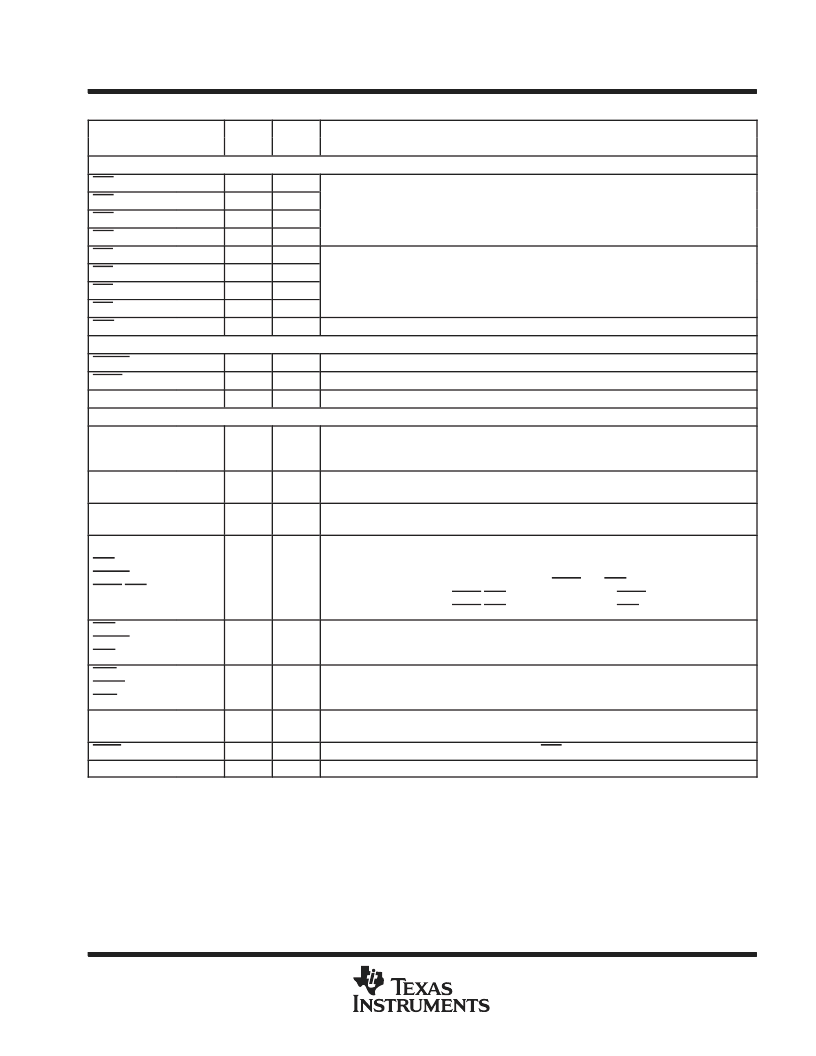
Terminal Functions (Continued)
SIGNAL
TYPE
IPD/
IPU
DESCRIPTION
NAME
NO.
EMIF (32-bit) CONTROL SIGNALS COMMON TO ALL TYPES OF MEMORY§
O/Z
IPU
EMIF memory space enables
O/Z
IPU
O/Z
IPU
CE3
L26
CE2
K23
O/Z
IPU
CE1
K24
Enabled by bits 28 through 31 of the word address
Only one pin is asserted during any external data access
CE0
K25
BE3
M25
O/Z
IPU
EMIF byte-enable control
Decoded from the low-order address bits. The number of address bits or byte enables
used depends on the width of external memory.
Byte-write enables for most types of memory
Can be directly connected to SDRAM read and write mask signal (SDQM)
EMIF peripheral data transfer, allows direct transfer between external peripherals
EMIF (32-BIT) BUS ARBITRATION§
BE2
M26
O/Z
IPU
BE1
L23
O/Z
IPU
BE0
L24
O/Z
IPU
PDT
M22
O/Z
IPU
HOLDA
N22
O
IPU
EMIF hold-request-acknowledge to the host
HOLD
V23
I
IPU
EMIF hold request from the host
BUSREQ
P22
O
IPU
EMIF bus request output
EMIF (32-BIT) ASYNCHRONOUS/SYNCHRONOUS MEMORY CONTROL§
ECLKIN
H25
I
IPD
EMIF external input clock. The EMIF input clock (ECLKIN, CPU/4 clock, or CPU/6 clock) is
selected at reset via the pullup/pulldown resistors on the ECLKIN_SEL[1:0] pins.
AECLKIN is the default for the EMIF input clock.
ECLKOUT2
J23
O/Z
IPD
EMIF output clock 2. Programmable to be EMIF input clock (ECLKIN, CPU/4 clock, or CPU/6
clock) frequency divided-by-1, -2, or -4.
ECLKOUT1
J26
O/Z
IPD
EMIF output clock 1 at EMIF input clock (ECLKIN, CPU/4 clock, or CPU/6 clock)
frequency.
ARE/
SDCAS/
SADS/SRE
J25
O/Z
IPU
EMIF asynchronous memory read-enable/SDRAM column-address strobe/programmable
synchronous interface-address strobe or read-enable
For programmable synchronous interface, the RENEN field in the CE Space Secondary
Control Register (CExSEC) selects between SADS and SRE:
If RENEN = 0, then the SADS/SRE signal functions as the SADS signal.
If RENEN = 1, then the SADS/SRE signal functions as the SRE signal.
AOE/
SDRAS/
SOE
J24
O/Z
IPU
EMIF asynchronous memory output-enable/SDRAM row-address strobe/programmable
synchronous interface output-enable
AWE/
SDWE/
SWE
K26
O/Z
IPU
EMIF asynchronous memory write-enable/SDRAM write-enable/programmable
synchronous interface write-enable
SDCKE
L25
O/Z
IPU
EMIF SDRAM clock-enable (used for self-refresh mode).
If SDRAM is not in system, SDCKE can be used as a general-purpose output.
SOE3
R22
O/Z
IPU
EMIF synchronous memory output-enable for CE3 (for glueless FIFO interface)
ARDY
I = Input, O = Output, Z = High impedance, S = Supply voltage, GND = Ground
IPD = Internal pulldown, IPU = Internal pullup. (These IPD/IPU signal pins feature a 30-k
IPD or IPU resistor. To pull up a signal to the opposite
supply rail, a 1-k
resistor should be used, unless otherwise noted.)
§To maintain signal integrity for the EMIF signals, serial termination resistors should be inserted into all EMIF output signal lines.
L22
I
IPU
Asynchronous memory ready input
相關PDF資料 |
PDF描述 |
|---|---|
| TMS32C6411AGLZ | FIXED POINT DIGITAL SIGNAL PROCESSOR |
| TMS32C6411AZLZ | FIXED POINT DIGITAL SIGNAL PROCESSOR |
| TMS32C6411GLZ | FIXED POINT DIGITAL SIGNAL PROCESSOR |
| TMS32C6411ZLZ | FIXED POINT DIGITAL SIGNAL PROCESSOR |
| TMX320C6411AGLZ | FIXED POINT DIGITAL SIGNAL PROCESSOR |
相關代理商/技術參數(shù) |
參數(shù)描述 |
|---|---|
| TMP34092PQL-64 | 制造商:Texas Instruments 功能描述: |
| TMP35FS | 制造商:Analog Devices 功能描述:Temp Sensor Analog(Voltage) Serial (2-Wire) 8-Pin SOIC N 制造商:Rochester Electronics LLC 功能描述:3V TEMPERATURE SENSOR - Bulk |
| TMP35FS-REEL | 制造商:Analog Devices 功能描述:Temp Sensor Analog Serial (2-Wire) 8-Pin SOIC N T/R 制造商:Rochester Electronics LLC 功能描述:3V TEMPERATURE SENSOR TAPE & REEL - Tape and Reel |
| TMP35FSZ | 制造商:Analog Devices 功能描述:Temperature Sensor IC |
| TMP35FSZ-REEL | 制造商:Analog Devices 功能描述:TEMP SENSOR ANLG SERL 8SOIC N - Tape and Reel |
發(fā)布緊急采購,3分鐘左右您將得到回復。