- 您現(xiàn)在的位置:買賣IC網(wǎng) > PDF目錄383942 > TE28F160S3-120 (INTEL CORP) 16 Characters x 2 Lines, 5x7 Dot Matrix Character and Cursor PDF資料下載
參數(shù)資料
| 型號: | TE28F160S3-120 |
| 廠商: | INTEL CORP |
| 元件分類: | DRAM |
| 英文描述: | 16 Characters x 2 Lines, 5x7 Dot Matrix Character and Cursor |
| 中文描述: | 1M X 16 FLASH 2.7V PROM, 120 ns, PDSO56 |
| 封裝: | 14 X 20 MM, TSOP-56 |
| 文件頁數(shù): | 25/52頁 |
| 文件大小: | 1262K |
| 代理商: | TE28F160S3-120 |
第1頁第2頁第3頁第4頁第5頁第6頁第7頁第8頁第9頁第10頁第11頁第12頁第13頁第14頁第15頁第16頁第17頁第18頁第19頁第20頁第21頁第22頁第23頁第24頁當(dāng)前第25頁第26頁第27頁第28頁第29頁第30頁第31頁第32頁第33頁第34頁第35頁第36頁第37頁第38頁第39頁第40頁第41頁第42頁第43頁第44頁第45頁第46頁第47頁第48頁第49頁第50頁第51頁第52頁
E
28F160S3, 28F320S3
25
ADVANCE INFORMATION
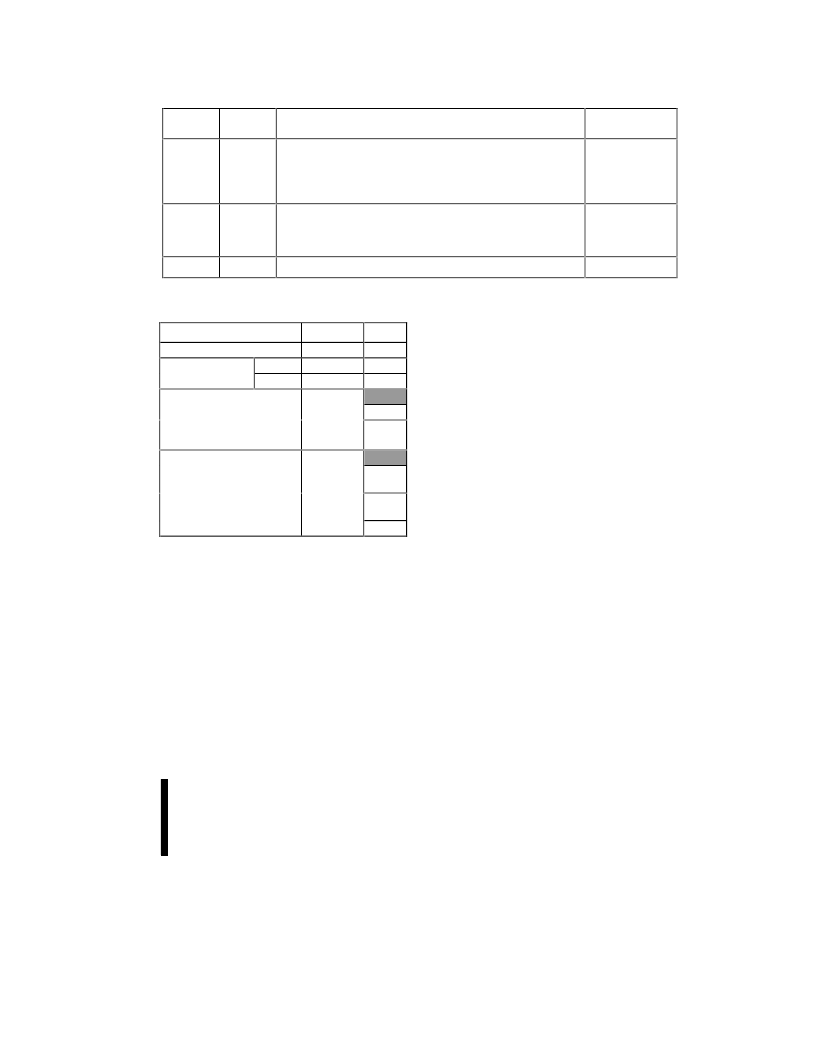
Table 11. Primary-Vendor Specific Extended Query
(Continued)
Offset
Length
(bytes)
Description
Data
(P+C)h
01h
V
CC
Logic Supply Optimum Program/Erase voltage (highest
performance)
bits 7
–4
bits 3–0
BCD value in volts
BCD value in 100 mv
3D:
0050h
(P+D)h
01h
V
PP
[Programming] Supply Optimum Program/Erase voltage
bits 7–4
bits 3–0
HEX value in volts
BCD value in 100 mv
3E:
0050h
(P+E)h
reserved
Reserved for future use
Table 12. Identifier Codes
Code
Address
(2)
000000
000001
000001
X
0002
(1)
Data
B0
D0
D4
Manufacturer Code
Device Code
16 Mbit
32 Mbit
Block Lock Configuration
Block is Unlocked
Block is Locked
Reserved for Future Use
Block Erase Status
Last erase completed
successfully
Last erase did not
complete successfully
Reserved for Future Use
NOTES:
1.
X selects the specific block lock configuration code.
See Figure 6 for the device identifier code memory
map.
2.
A
should be ignored in this address. The lowest order
address line is A
1
in both word and byte mode.
DQ
0
= 0
DQ
0
= 1
DQ
2-7
x0002
(1)
DQ
1
= 0
DQ
1
= 1
DQ
2-7
4.3
Read Identifier Codes
Command
The identifier code operation is initiated by writing
the Read Identifier Codes command. Following the
command write, read cycles from addresses shown
in Figure 6 retrieve the manufacturer, device, block
lock configuration, and block erase status codes
(see Table 12 for identifier code values). To
terminate the operation, write another valid
command. Like the Read Array command, the
Read
Identifier
Codes
independently of the V
voltage. Following the
Read Identifier Codes command, the information in
Table 12 can be read.
command
functions
4.4
Read Status Register
Command
The Status Register may be read to determine
when programming, block erasure, or lock-bit
configuration is complete and whether the operation
completed successfully. It may be read at any time
by writing the Read Status Register command.
After writing this command, all subsequent read
operations output data from the Status Register
until another valid command is written. The Status
Register contents are latched on the falling edge of
OE#, CE
0
#, or CE
1
# whichever occurs last. OE# or
CE
X
# must toggle to V
IH
to update the Status
Register latch. The Read Status Register command
functions independently of the V
PP
voltage.
相關(guān)PDF資料 |
PDF描述 |
|---|---|
| TE28F400B3T90 | 3 Volt Advanced Boot Block Flash Memory |
| TE28F004 | 3 Volt Advanced Boot Block Flash Memory |
| TE28F004B3T90 | 3 Volt Advanced Boot Block Flash Memory |
| TE28F640B3TC100 | 3 Volt Advanced Boot Block Flash Memory |
| TE28F320B3TC70 | 3 Volt Advanced Boot Block Flash Memory |
相關(guān)代理商/技術(shù)參數(shù) |
參數(shù)描述 |
|---|---|
| TE28F160S3-130 | 制造商:INTEL 制造商全稱:Intel Corporation 功能描述:WORD-WIDE FlashFile MEMORY FAMILY |
| TE28F160S3-75 | 制造商:INTEL 制造商全稱:Intel Corporation 功能描述:WORD-WIDE FlashFile MEMORY FAMILY |
| TE28F160S375-RFB | 制造商:Intel 功能描述: |
| TE28F200B5B80 | 制造商:Intel 功能描述: |
| TE28F200B5T80 | 制造商:INTEL 制造商全稱:Intel Corporation 功能描述:SMART 5 BOOT BLOCK FLASH MEMORY FAMILY 2, 4, 8 MBIT |
發(fā)布緊急采購,3分鐘左右您將得到回復(fù)。