- 您現(xiàn)在的位置:買賣IC網(wǎng) > PDF目錄383991 > TE28F160B3B90 (INTEL CORP) SMART 3 ADVANCED BOOT BLOCK 4-, 8-, 16-, 32-MBIT FLASH MEMORY FAMILY PDF資料下載
參數(shù)資料
| 型號(hào): | TE28F160B3B90 |
| 廠商: | INTEL CORP |
| 元件分類: | DRAM |
| 英文描述: | SMART 3 ADVANCED BOOT BLOCK 4-, 8-, 16-, 32-MBIT FLASH MEMORY FAMILY |
| 中文描述: | 1M X 16 FLASH 2.7V PROM, 90 ns, PDSO48 |
| 封裝: | 12 X 20 MM, TSOP-48 |
| 文件頁(yè)數(shù): | 10/48頁(yè) |
| 文件大小: | 304K |
| 代理商: | TE28F160B3B90 |
第1頁(yè)第2頁(yè)第3頁(yè)第4頁(yè)第5頁(yè)第6頁(yè)第7頁(yè)第8頁(yè)第9頁(yè)當(dāng)前第10頁(yè)第11頁(yè)第12頁(yè)第13頁(yè)第14頁(yè)第15頁(yè)第16頁(yè)第17頁(yè)第18頁(yè)第19頁(yè)第20頁(yè)第21頁(yè)第22頁(yè)第23頁(yè)第24頁(yè)第25頁(yè)第26頁(yè)第27頁(yè)第28頁(yè)第29頁(yè)第30頁(yè)第31頁(yè)第32頁(yè)第33頁(yè)第34頁(yè)第35頁(yè)第36頁(yè)第37頁(yè)第38頁(yè)第39頁(yè)第40頁(yè)第41頁(yè)第42頁(yè)第43頁(yè)第44頁(yè)第45頁(yè)第46頁(yè)第47頁(yè)第48頁(yè)
SMART 3 ADVANCED BOOT BLOCK
E
10
PRELIMINARY
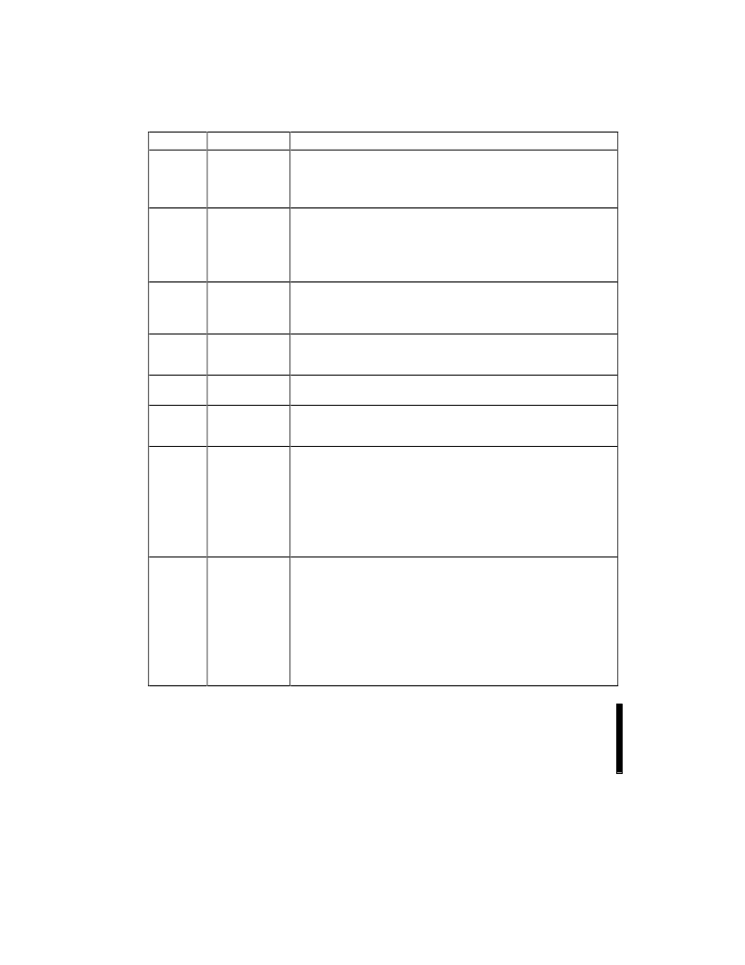
The pin descriptions table details the usage of each device pin.
Table 2. Smart 3 Advanced Boot Block Pin Descriptions
Symbol
Type
Name and Function
A
0
–A
21
INPUT
ADDRESS INPUTS
for memory addresses. Addresses are internally
latched during a program or erase cycle.
28F008B3: A[0-19], 28F016B3: A[0-20], 28F032B3: A[0-21],
28F800B3: A[0-17], 28F800B3: A[0-18], 28F160B3: A[0-19],
28F320B3: A[0-20]
DATA INPUTS/OUTPUTS:
Inputs array data on the second CE# and
WE# cycle during a Program command. Inputs commands to the
Command User Interface when CE# and WE# are active. Data is
internally latched. Outputs array, identifier and status register data. The
data pins float to tri-state when the chip is de-selected or the outputs are
disabled.
DQ
0
–DQ
7
INPUT/OUTPUT
DQ
8
–DQ
15
INPUT/OUTPUT
DATA INPUTS/OUTPUTS:
Inputs array data on the second CE# and
WE# cycle during a Program command. Data is internally latched.
Outputs array and identifier data. The data pins float to tri-state when the
chip is de-selected.
Not included on x8 products.
CE#
INPUT
CHIP ENABLE:
Activates the internal control logic, input buffers,
decoders and sense amplifiers. CE# is active low. CE# high de-selects
the memory device and reduces power consumption to standby levels.
OE#
INPUT
OUTPUT ENABLE:
Enables the device’s outputs through the data
buffers during a read operation. OE# is active low.
WE#
INPUT
WRITE ENABLE:
Controls writes to the Command Register and memory
array. WE# is active low. Addresses and data are latched on the rising
edge of the second WE# pulse.
RP#
INPUT
RESET/DEEP POWER-DOWN:
Uses two voltage levels (V
IL
, V
IH
) to
control reset/deep power-down mode.
When RP# is at logic low, the device is in reset/deep power-down
mode
, which drives the outputs to High-Z, resets the Write State
Machine, and minimizes current levels (I
CCD
).
When RP# is at logic high, the device is in standard operation
.
When RP# transitions from logic-low to logic-high, the device resets all
blocks to locked and defaults to the read array mode.
WP#
INPUT
WRITE PROTECT:
Provides a method for locking and unlocking the two
lockable parameter blocks.
When WP# is at logic low, the lockable blocks are locked
,
preventing program and erase operations to those blocks. If a program
or erase operation is attempted on a locked block, SR.1 and either SR.4
[program] or SR.5 [erase] will be set to indicate the operation failed.
When WP# is at logic high, the lockable blocks are unlocked
and
can be programmed or erased.
See Section 3.3 for details on write protection.
相關(guān)PDF資料 |
PDF描述 |
|---|---|
| TE28F032B3B90 | TVS UNIDIRECT 400W 78V SMA |
| TE28F320B3BA110 | SMART 3 ADVANCED BOOT BLOCK 4-, 8-, 16-, 32-MBIT FLASH MEMORY FAMILY |
| TE28F016 | SMART 3 ADVANCED BOOT BLOCK 4-, 8-, 16-, 32-MBIT FLASH MEMORY FAMILY |
| TE28F160B3T110 | SMART 3 ADVANCED BOOT BLOCK 4-, 8-, 16-, 32-MBIT FLASH MEMORY FAMILY |
| TE28F160C3 | 3 Volt Intel Advanced+ Boot Block Flash Memory |
相關(guān)代理商/技術(shù)參數(shù) |
參數(shù)描述 |
|---|---|
| TE28F160B3BA110 | 制造商:Intel 功能描述:NOR Flash, 1M x 16, 48 Pin, Plastic, TSSOP |
| TE28F160B3BA110S | 制造商:Rochester Electronics LLC 功能描述:- Bulk 制造商:Intel 功能描述: |
| TE28F160B3BA90 | 制造商:INTEL 制造商全稱:Intel Corporation 功能描述:3 Volt Advanced Boot Block Flash Memory |
| TE28F160B3BC70 | 制造商:INTEL 制造商全稱:Intel Corporation 功能描述:3 Volt Advanced Boot Block Flash Memory |
| TE28F160B3BC80 | 制造商:INTEL 制造商全稱:Intel Corporation 功能描述:3 Volt Advanced Boot Block Flash Memory |
發(fā)布緊急采購(gòu),3分鐘左右您將得到回復(fù)。