- 您現(xiàn)在的位置:買賣IC網(wǎng) > PDF目錄383989 > TDA4885 (NXP SEMICONDUCTORS) 150 MHz video controller with I2C-bus PDF資料下載
參數(shù)資料
| 型號: | TDA4885 |
| 廠商: | NXP SEMICONDUCTORS |
| 元件分類: | 消費家電 |
| 英文描述: | 150 MHz video controller with I2C-bus |
| 中文描述: | SPECIALTY CONSUMER CIRCUIT, PDIP32 |
| 封裝: | 0.400 INCH, PLASTIC, SOT-232-1, SDIP-32 |
| 文件頁數(shù): | 16/56頁 |
| 文件大?。?/td> | 396K |
| 代理商: | TDA4885 |
第1頁第2頁第3頁第4頁第5頁第6頁第7頁第8頁第9頁第10頁第11頁第12頁第13頁第14頁第15頁當前第16頁第17頁第18頁第19頁第20頁第21頁第22頁第23頁第24頁第25頁第26頁第27頁第28頁第29頁第30頁第31頁第32頁第33頁第34頁第35頁第36頁第37頁第38頁第39頁第40頁第41頁第42頁第43頁第44頁第45頁第46頁第47頁第48頁第49頁第50頁第51頁第52頁第53頁第54頁第55頁第56頁
1997 Nov 25
16
Philips Semiconductors
Product specification
150 MHz video controller with I
2
C-bus
TDA4885
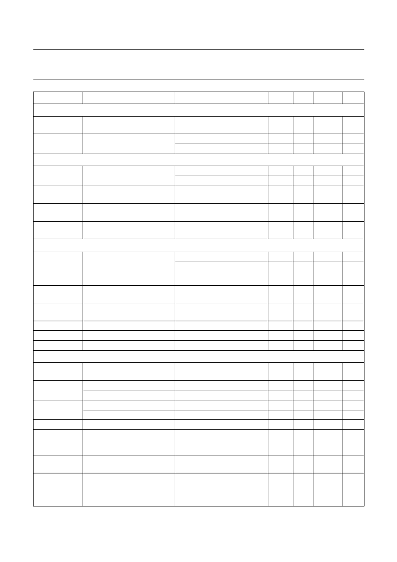
Crosstalk at signal outputs (channel 1: pin 30; channel 2: pin 25; channel 3: pin 20)
α
ct(tr)
transient crosstalk suppression input rise/fall time = 1 ns;
note 26
f = 50 MHz
f = 100 MHz
10
25
dB
α
ct(f)
crosstalk suppression by
frequency
25
10
30
20
dB
dB
Internal feedback reference voltage;
see Fig.15 and note 27
V
ref(n)
internal reference voltage for
negative feedback polarity
FFH; FPOL = 0
00H; FPOL = 0
FPOL = 1
3.8
5.6
0.6
4.0
5.8
0.7
4.2
6.1
0.8
V
V
V
V
ref(p)
fixed internal reference voltage
for positive feedback polarity
variation of V
ref(n)
and V
ref(p)
in
the temperature range
variation of V
ref(n)
and V
ref(p)
with supply voltage V
P
V
ref
/
T
T
amb
=
20 to +70
°
C
0
±
1.0
%
V
ref
/
V
P
7.6 V
≤
V
P
≤
8.8 V
0
±
1.0
%
External reference voltages (REF
1
: pin 32; REF
2
: pin 27; REF
3
: pin 22);
see Fig.16 and note 28
V
32, 27, 22
external reference voltage
(equal to internal reference
voltage with control bit
FPOL = 0 )
variation of V
32, 27, 22
in the
temperature range
variation of V
32, 27, 22
with
supply voltage V
P
output resistance
maximum sink current
maximum source current
FFH
00H
3.8
5.6
4.0
5.8
4.2
6.1
V
V
V
32, 27, 22
/
T
T
amb
=
20 to +70
°
C
0
±
1.0
%
V
32, 27, 22
/
V
P
7.6 V
≤
V
P
≤
8.8 V
0
±
1.0
%
R
32, 27, 22
I
32, 27, 22
I
32, 27, 22
90
330
400
280
μ
A
μ
A
Output clamping, feedback inputs (channel 1: pin 31; channel 2: pin 26; channel 3: pin 21)
I
31, 26, 21(max)
maximum input current
during output clamping;
V
11
> 3.5 V; V
31, 26, 21
= 0.5 V
PEDST = 0; V
11
> 3.5 V
PEDST = 1; V
11
> 3.5 V
500
100
60
nA
V
30, 25, 20rbl(min)
minimum reference black level
minimum pedestal black level
maximum reference black level PEDST = 0; V
11
> 3.5 V
maximum pedestal black level
black level variation at CRT
black level variation between
clamping pulses related to
nominal colour signal
width of clamping pulse
0.01
0.01
2.4
2.4
0
0.1
0.1
2.8
2.8
40
0.1
0.5
0.5
4
4
200
0.5
V
V
V
V
mV
%
V
30, 25, 20rbl(max)
PEDST = 1; V
11
> 3.5 V
note 29
line frequency 60 kHz;
10% duty cycle
V
bl(CRT)
V
bl(lf)
t
W11
measured at V
11
= 3 V;
see Fig.8
see Fig.8
1
μ
s
t
d11(clamp)l
delay between clamping input
at pin 11 (leading edge) and
start of internal output clamping
pulse
300
ns
SYMBOL
PARAMETER
CONDITIONS
MIN.
TYP.
MAX.
UNIT
相關(guān)PDF資料 |
PDF描述 |
|---|---|
| TDA4886A | 140 MHz video controller with I2C-bus |
| TDA4886 | 140 MHz video controller with I2C-bus |
| TDA4887 | 160 MHz bus-controlled monitor video preamplifier |
| TDA4887PS | 160 MHz bus-controlled monitor video preamplifier |
| TDA5140 | Transient Voltage Suppressor Diodes |
相關(guān)代理商/技術(shù)參數(shù) |
參數(shù)描述 |
|---|---|
| TDA4885/V2 | 制造商:NXP Semiconductors 功能描述: |
| TDA4886 | 制造商:PHILIPS-SEMI 功能描述: |
| TDA4886A | 制造商:PHILIPS 制造商全稱:NXP Semiconductors 功能描述:140 MHz video controller with I2C-bus |
| TDA4887 | 制造商:PHILIPS 制造商全稱:NXP Semiconductors 功能描述:160 MHz bus-controlled monitor video preamplifier |
| TDA4887PS | 制造商:PHILIPS 制造商全稱:NXP Semiconductors 功能描述:160 MHz bus-controlled monitor video preamplifier |
發(fā)布緊急采購,3分鐘左右您將得到回復。