- 您現(xiàn)在的位置:買賣IC網(wǎng) > PDF目錄371180 > T8531A T8531A/8532 Multichannel Programmable Codec Chip Set PDF資料下載
參數(shù)資料
| 型號: | T8531A |
| 元件分類: | Codec |
| 英文描述: | T8531A/8532 Multichannel Programmable Codec Chip Set |
| 中文描述: | T8531A/8532多通道可編程解碼器芯片組 |
| 文件頁數(shù): | 44/50頁 |
| 文件大小: | 888K |
| 代理商: | T8531A |
第1頁第2頁第3頁第4頁第5頁第6頁第7頁第8頁第9頁第10頁第11頁第12頁第13頁第14頁第15頁第16頁第17頁第18頁第19頁第20頁第21頁第22頁第23頁第24頁第25頁第26頁第27頁第28頁第29頁第30頁第31頁第32頁第33頁第34頁第35頁第36頁第37頁第38頁第39頁第40頁第41頁第42頁第43頁當(dāng)前第44頁第45頁第46頁第47頁第48頁第49頁第50頁
44
Agere Systems Inc.
Preliminary Data Sheet
September 2001
Codec Chip Set
T8531A/T8532 Multichannel Programmable
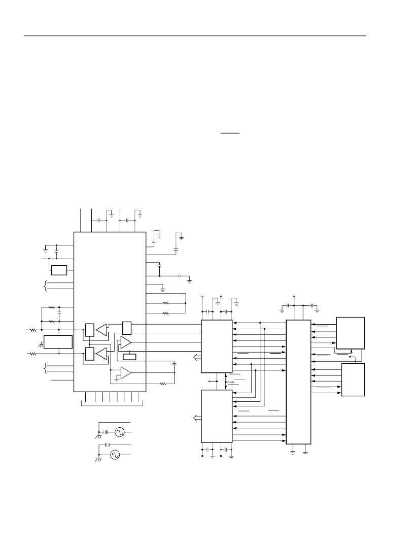
Applications
Figure 11 shows a full line card implementation using the T8531/T8532 codec and the L7585 SLIC with integrated
relays. One T8531A and two T8532 devices support 16 SLIC devices (only one L7585 SLIC is illustrated). Figure
11 portrays only the transmission paths inside the L7585 SLIC. L7585 functionality includes eight solid-state relays,
performing ring, test, and break functions, a ring-trip detector, quiet polarity reversal, 14 operating states, and
more. For complete functionality of this SLIC, refer to the L7585 data sheet.
The analog connection between the SLIC and the codec is direct; no external components are required. The trans-
fer of control data on the octal interface between the T8531A and T8532 devices is also direct. Data is synchro-
nous with OSCK and transmits at a 4.096 MHz rate. The microprocessor control interface is a standard 4-wire
serial port connection, microprocessor clock (UPCK), chip select (UPCS), data input (UPDI), and output (UPDO).
The T8531A generates a 16 MHz clock for microprocessor use. This clock is always present. The PCM interface
consists of a system clock (SCK) input of either 2.048 MHz or 4.096 MHz, an 8 kHz system frame sync (SFS)
input, a system data transmit port (DX), and a system data receive (DR) port.
The only external components required by the codec chip set are the power supply decoupling. Decouple as many
power supply pins as possible, at a minimum, use one capacitor per device side. Analog and digital grounds should
be tied together into one low-impedance ground plane.
12-3351p(F)
* Optional for quiet reverse battery.
4.096 MHz operation; for 2.048 MHz operation, tie SCKSEL to V
SS
.
Figure 11. Line Card Solution Using the L7585 SLIC
OSFS
OSCK
OSDR0
OSDR1
OSDX0
OSDX1
CCS0
CDO
CDI
CT8532
DSP
ASIC
UPCK
UPCS
UPDI
UPDO
CK16
SCK
SFS
SDR
SDX
STSXB
PCM
BUS
T8532
OSDX2
OSDX3
OSDR2
OSDR3
PCM
INTERFACE
ICONTROL
OCTAL
INTERFACE
OSDX2
OSDX3
OSDR2
OSDR3
CDO
OSFS
CDI
OSCK
OSFS
OSCK
OSDR0
OSDR1
OSDX0
OSDX1
CCS0
CDI
CDO
CCS1
CCS1
DGND
VCCD
RDO
RSW
RTS
PR
PT
RTI
TTI
CLK
VSP VBAT
BGND VCCA AGND
NDET NCSB5 B4 B3 B2 B1 B0
FB1
FB2
CF1
CF2
DCR
DCOUT
IPROG
LCTH
RCVN
RCVP
VTX
VRTX
TXI
VITR
ITR
RK1
CVD
μ
F
CRTF
μ
F
50 V
RS1
1 M
260 V
SURGE
PROTECTOR
RPR
82.5
RPT
TEBUS
1 MHz
BATTERY BACK
RINGING
CVB
0.1
μ
F
–48 V
CVA
0.1
μ
F
+5 V
+10 V
FB2*
μ
F
100 V
CF1
0.22
μ
F
100 V
CF2
0.1
μ
F
100 V
RPROG 64.9 k
RLCTH 24.9 k
+5 V
CB1
μ
F
100 V
L7585
PARALLEL DATA BUS TO MICROPROCESSOR
0.1
μ
F
+5 V
0.1
μ
F
+5 V
RSTB
SCKSEL
RSTB
0.1
μ
F
0.1
μ
F
CH8—15
CH1—7
+5 V
+5 V
CHA0
VRN0
VRP0
VTX0
VRTX0
TEST
TEST
VDDD
RSTB
RSTB
RSTB
VSS
VSSA
0.1
μ
F
+5 V
0.1
μ
F
VDD
2.4 V
RGX1
8.25 k
TIP
RING
FB1*
μ
F
100 V
V
V
V
V
V
V
V
V
VDDA
PRMICRO-
T8531A
10 V
TRNG
RRNG
EARTH BACK
RINGING
TRNG
RRNG
TRNG
RRNG
RINGING
BUS
(SEE BELOW)
100 V
相關(guān)PDF資料 |
PDF描述 |
|---|---|
| T8531 | T8502 and T8503 Dual PCM Codecs with Filters |
| T8532 | T8502 and T8503 Dual PCM Codecs with Filters |
| T8533 | T8533/34 Quad Programmable Line Card Signal Processor |
| T8534 | T8533/34 Quad Programmable Line Card Signal Processor |
| T8535B | T8535B/T8536B Quad Programmable Codec |
相關(guān)代理商/技術(shù)參數(shù) |
參數(shù)描述 |
|---|---|
| T8532 | 制造商:AGERE 制造商全稱:AGERE 功能描述:T8531A/8532 Multichannel Programmable Codec Chip Set |
| T8533 | 制造商:AGERE 制造商全稱:AGERE 功能描述:T8533/34 Quad Programmable Line Card Signal Processor |
| T85331G | 制造商:BITECH 制造商全稱:Bi technologies 功能描述:Thick Film Super Low Profile SIP Resistor Networks |
| T85331J | 制造商:BITECH 制造商全稱:Bi technologies 功能描述:Thick Film Super Low Profile SIP Resistor Networks |
| T8534 | 制造商:AGERE 制造商全稱:AGERE 功能描述:T8533/34 Quad Programmable Line Card Signal Processor |
發(fā)布緊急采購,3分鐘左右您將得到回復(fù)。