- 您現(xiàn)在的位置:買賣IC網(wǎng) > PDF目錄383835 > SSTV16857MTDX Memory Driver PDF資料下載
參數(shù)資料
| 型號(hào): | SSTV16857MTDX |
| 元件分類: | 通用總線功能 |
| 英文描述: | Memory Driver |
| 中文描述: | 記憶體驅(qū)動(dòng) |
| 文件頁(yè)數(shù): | 3/6頁(yè) |
| 文件大小: | 76K |
| 代理商: | SSTV16857MTDX |
3
www.fairchildsemi.com
S
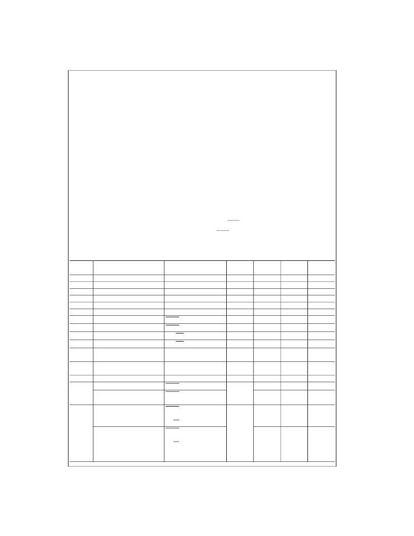
Absolute Maximum Ratings
(Note 1)
Recommended Operating
Conditions
(Note 3)
Note 1:
The
“
Absolute Maximum Ratings
”
are those values beyond which
the safety of the device cannot be guaranteed. The device should not be
operated at these limits. The parametric values defined in the
“
Electrical
Characteristics
”
table are not guaranteed at the absolute maximum ratings.
The
“
Recommended Operating Conditions
”
table will define the conditions
for actual device operation.
Note 2:
IO Absolute Maximum Rating must be observed.
Note 3:
The RESET input of the device must be held at V
DD
or GND to
ensure proper device operation. The differential inputs must not be floating,
unless RESET is asserted LOW.
DC Electrical Characteristics
(2.3V
≤
V
DD
≤
2.7V)
Supply Voltage (V
DDQ
)
Supply Voltage (V
DD
)
Reference Voltage (V
REF
)
Input Voltage (V
I
)
Output Voltage (V
O
)
Outputs Active (Note 2)
DC Input Diode Current (I
IK
)
V
I
<
0V
V
I
>
V
DD
DC Output Diode Current (I
OK
)
V
O
<
0V
V
O
>
V
DD
DC Output Source/Sink Current
(I
OH
/I
OL
)
DC V
DD
or Ground Current
per Supply Pin (I
DD
or Ground)
Storage Temperature Range (T
stg
)
0.5V to
+
3.6V
0.5V to
+
3.6V
0.5V to
+
3.6V
0.5V to V
DD
+
0.5V
0.5V to V
DDQ
+
0.5V
50 mA
+
50 mA
50 mA
+
50 mA
±
50 mA
±
100 mA
65
°
C to
+
150
°
C
Power Supply (V
DDQ
)
Power Supply (V
DD
)
Operating Range
Reference Supply
(V
REF
=
V
DDQ
/2)
Termination Voltage (V
TT
)
Input Voltage
Output Voltage (V
O
)
Output in Active States
Output Current I
OH
/I
OL
V
DD
=
2.3V to 2.7V
Free Air Operating Temperature (T
A
)
2.3V to 2.7V
V
DDQ
to 2.7V
1.15 to 1.35
V
REF
±
40 mV
0V to V
DD
0V to V
DDQ
±
20 mA
0
°
C to
+
70
°
C
Symbol
Parameter
Conditions
V
DD
(V)
2.3
Min
Max
Units
V
IKL
V
IKH
V
IH-AC
V
IL-AC
V
IH-DC
V
IL-DC
Input LOW Clamp Voltage
I
I
=
18 mA
I
I
=
+
18 mA
Data Inputs
Data Inputs
1.2
3.5
V
Input HIGH Clamp Voltage
AC HIGH Level Input Voltage
AC LOW Level Input Voltage
2.3
V
V
V
V
REF
+
310mV
V
REF
310mV
DC HIGH Level Input Voltage
DC LOW Level Input Voltage
Data Inputs
Data Inputs
V
REF
+
150mV
V
V
V
REF
150mV
V
IH
HIGH Level Input Voltage
RESET
1.7
V
V
IL
LOW Level Input Voltage
RESET
0.7
V
V
ICR
Common Mode Input Voltage Range
CLK, CLK
0.97
1.53
V
V
I(PP)
V
OH
Peak to Peak Input Voltage
HIGH Level Output Voltage
CLK, CLK
I
OH
=
100
μ
A
I
OH
=
16 mA
I
OL
=
100
μ
A
I
OL
=
16 mA
V
I
=
V
DD
or GND
360
mV
2.3 to 2.7
V
DD
0.2
1.95
V
2.3
V
OL
LOW Level Output Voltage
2.3 to 2.7
2.3
0.2
0.35
±
5.0
V
I
I
Input Leakage Current
2.7
μ
A
I
DD
Static Standby
RESET
=
GND, I
O
=
0
2.7
10
μ
A
Static Operating
RESET
=
V
DD
, I
O
=
0
V
I
=
V
IH(AC)
or V
IL(AC)
25
mA
I
DDD
Dynamic Operating Current
Clock Only
RESET
=
V
DD
, I
O
=
0
V
I
=
V
IH(AC)
or V
IL(AC)
CK, CK Duty Cycle 50%
2.7
μ
A/MHz
90
Dynamic Operating Current
per Data Input
RESET
=
V
DD
, I
O
=
0
V
I
=
V
IH(AC)
or V
IL(AC)
CK, CK Duty Cycle 50%
Data Input
=
Clock
Rate 50% Duty Cycle
μ
A/MHz
15
相關(guān)PDF資料 |
PDF描述 |
|---|---|
| SSTV16859DGG | IC CLOCK BUFFER TTL OUT 32-PLCC |
| SSTV16859GX | Memory Driver |
| SSTV16859MTDX | 1-Mbit (64K x 16) Static RAM |
| SSTV16859 | Dual Output 13-Bit Register with SSTL-2 Compatible I/O and Reset |
| SSTV16859G | Voltage Regulator IC; Output Current:300mA; Package/Case:8-MSOP; Supply Voltage Max:6V; Current Rating:300mA; Leaded Process Compatible:No; Output Current Max:300mA; Output Voltage Max:5V; Output Voltage Min:1.215V |
相關(guān)代理商/技術(shù)參數(shù) |
參數(shù)描述 |
|---|---|
| SSTV16857MTDX_NL | 功能描述:寄存器 14-Bit Register with SSTL-2 Compatible I/O and Reset RoHS:否 制造商:NXP Semiconductors 邏輯類型:CMOS 邏輯系列:HC 電路數(shù)量:1 最大時(shí)鐘頻率:36 MHz 傳播延遲時(shí)間: 高電平輸出電流:- 7.8 mA 低電平輸出電流:7.8 mA 電源電壓-最大:6 V 最大工作溫度:+ 125 C 封裝 / 箱體:SOT-38 封裝:Tube |
| SSTV16857TE-E | 制造商:Renesas Electronics Corporation 功能描述:14-BIT SSTL_2 REGISTERED BUFFER TSSOP 48 PIN - Tape and Reel |
| SSTV16859 | 制造商:PHILIPS 制造商全稱:NXP Semiconductors 功能描述:2.5 V 13-bit to 26-bit SSTL_2 registered buffer for stacked DDR DIMM |
| SSTV16859_ZAA31162 WAF | 制造商:Fairchild Semiconductor Corporation 功能描述: |
| SSTV16859_ZBA30062 WAF | 制造商:Fairchild Semiconductor Corporation 功能描述: |
發(fā)布緊急采購(gòu),3分鐘左右您將得到回復(fù)。