- 您現(xiàn)在的位置:買賣IC網(wǎng) > PDF目錄98081 > SK12439PJT 800 MHz, OTHER CLOCK GENERATOR, PQCC28 PDF資料下載
參數(shù)資料
| 型號: | SK12439PJT |
| 元件分類: | 時鐘產(chǎn)生/分配 |
| 英文描述: | 800 MHz, OTHER CLOCK GENERATOR, PQCC28 |
| 封裝: | PLASTIC, LCC-28 |
| 文件頁數(shù): | 15/18頁 |
| 文件大?。?/td> | 233K |
| 代理商: | SK12439PJT |
6
Revision 1/February 9, 2001
www.semtech.com
HIGH-PER.ORMANCE PRODUCTS
SK12439
ADVANCED
Application Information (continued)
The TEST output provides visibility for one of the several
internal nodes as determined by the T[2:0] bits in the
serial configuration stream. It is not configurable through
the parallel interface. Although it is possible to select the
node that represents FOUT, the CMOS output may not be
able to toggle fast enough for some of the higher output
frequencies. The T2, T1, and T0 control bits are present
to ‘000’ when P_LOAD* is LOW so that the PECL FOUT
outputs are as jitter-free as possible. Any active signal on
the TEST output pin will have detrimental affects on the
jitter of the PECL output pair. In normal operations, jitter
specifications are only guaranteed if the TEST output is
static. The serial configuration port can be used to select
one of the alternate functions for this pin.
Most of the signals available on the TEST output pin are
useful only for performance verification of the SK12439
itself. However, the PLL bypass mode may be of interest
at the board level for functional debug. When T[2:0] is
set to 110, the SK12439 is placed in PLL bypass mode.
First Bit
Last Bit
T1
T0
N1
N0
M6
M5
M4
M3
M2
M1
M0
T2
M, N
S_CLOCK
S_DATA
S_LOAD
P_LOAD*
M[6:0]
N[1:0]
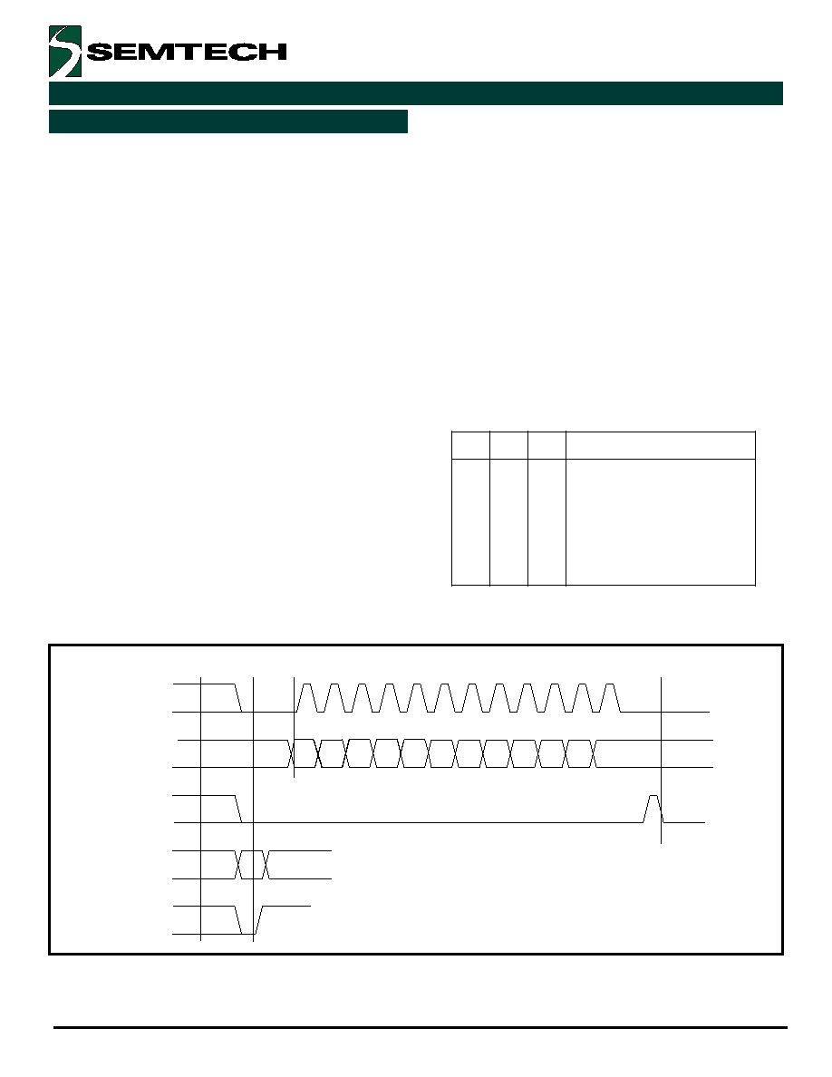
In this mode, the S_CLOCK input is fed directly into the M
and N dividers. The N divider drives the FOUT differential
pair and the M counter drives the TEST output pin. In this
mode, the S_CLOCK input could be used for low speed
board level functional test or debug. Bypassing the PLL
and driving FOUT directly gives the user more control on
the test clocks sent through the clock tree. Figure 4 shows
the functional setup of the PLL bypass mode. Because
the S_CLOCK is a CMOS level, the input frequency is lim-
ited to 250 MHz or less. This means the fastest the FOUT
pin can be toggled via the S_CLOCK is 250 MHz as the
minimum divide ratio of the N counter is 1. Note that the
M counter output on the TEST output will not be a 50%
duty cycle due to the way the divider is implemented.
2
T1
T0
T)
0
2
n
i
P
(
T
S
E
T
0
1
0
1
0
1
0
1
0
1
0
1
0
1
T
U
O
R
E
T
S
I
G
E
R
T
.
I
H
S
H
G
I
H
.
E
R
.
2
/
T
U
O
R
E
T
N
U
O
C
M
T
U
O
.
W
O
L
e
d
o
M
s
a
p
y
B
L
P
n
i
2
/
R
E
T
N
U
O
C
M
4
/
U
O
.
Figure 3.
Timing Diagram
相關(guān)PDF資料 |
PDF描述 |
|---|---|
| SL15100ZIT-XXX | 200 MHz, OTHER CLOCK GENERATOR, PDSO8 |
| SL15100ZCT-XXX | 200 MHz, OTHER CLOCK GENERATOR, PDSO8 |
| SL15102DI-XXX | OTHER CLOCK GENERATOR, DSO8 |
| SL15300EZCT-XXX | 200 MHz, OTHER CLOCK GENERATOR, PDSO8 |
| SL15300EZI-XXX | 200 MHz, OTHER CLOCK GENERATOR, PDSO8 |
相關(guān)代理商/技術(shù)參數(shù) |
參數(shù)描述 |
|---|---|
| SK125 | 制造商:Thomas & Betts 功能描述: |
| SK1250C | 制造商:DEC 制造商全稱:DEC 功能描述:12 AMP SCHOTTKY BARRIER RECTIFIERS |
| SK12516 | 制造商:Cooper Wiring Devices 功能描述: |
| SK1260C | 制造商:DEC 制造商全稱:DEC 功能描述:12 AMP SCHOTTKY BARRIER RECTIFIERS |
| SK1270C | 制造商:DEC 制造商全稱:DEC 功能描述:12 AMP SCHOTTKY BARRIER RECTIFIERS |
發(fā)布緊急采購,3分鐘左右您將得到回復(fù)。