- 您現(xiàn)在的位置:買賣IC網(wǎng) > PDF目錄374791 > SiI161ACT100 (Electronic Theatre Controls, Inc.) SiI 161A PanelLink Receiver PDF資料下載
參數(shù)資料
| 型號(hào): | SiI161ACT100 |
| 廠商: | Electronic Theatre Controls, Inc. |
| 英文描述: | SiI 161A PanelLink Receiver |
| 中文描述: | 精工161A條PanelLink接收機(jī) |
| 文件頁數(shù): | 3/22頁 |
| 文件大?。?/td> | 260K |
| 代理商: | SII161ACT100 |
S ilic on Image, Inc .
SiI 161
A
SiI
-DS-0009-D
S ilic on Image, Inc .
3
Subject to Change without Notice
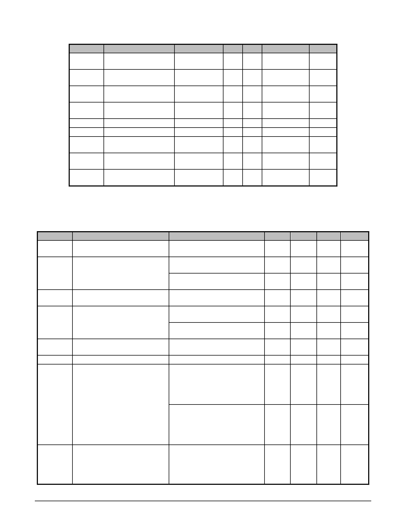
DC Digital I/O Specifications
Under normal operating conditions unless otherwise specified.
Symbol
Parameter
V
IH
High-level Input
Voltage
V
IL
Low-level Input
Voltage
V
OH
High-level Output
Voltage
V
OL
Low-level Output
Voltage
V
CINL
Input Clamp Voltage
1
V
CIPL
Input Clamp Voltage
1
V
CONL
Output Clamp
Voltage
1
V
COPL
Output Clamp
Voltage
1
I
OL
Output Leakage
Current
Note:
1
Guaranteed by design. Voltage undershoot or overshoot cannot exceed absolute maximum conditions for a pulse of
greater than 3 ns or one third of the clock cycle.
DC Specifications
Under normal operating conditions unless otherwise specified.
Symbol
Parameter
Conditions
I
OHD
Output High Drive Data and
Controls
I
OLD
Output Low Drive Data and
Controls
V
OUT
= 0.4 V;
I
OHC
ODCK, DE High Drive
V
OUT
= 2.4 V;
I
OLC
ODCK, DE Low Drive
V
OUT
= 0.8V; ST = 1
V
OUT
= 0.4 V;
V
ID
Differential Input Voltage
Single Ended Amplitude
I
PD
Power-down Current
2
I
CCR
Receiver Supply Current
2-pixel/clock mode
C
LOAD
= 10pF
R
EXT_SWING
= 510
Typical Pattern
3
ODCK=82.5MHz,
2-pixel/clock mode
C
LOAD
= 10pF
R
EXT_SWING
= 510
Worst Case Pattern
4
I
PDO
Receiver Supply Current with
Ouputs Powered Down
2-pixel/clock mode
C
LOAD
= 10pF
R
EXT_SWING
= 510
Worst Case Pattern
4
1
Guaranteed by design.
Conditions
Min
2
Typ
Max
Units
V
0.8
V
2.4
V
0.4
V
I
CL
= -18mA
I
CL
= 18mA
I
CL
= -18mA
GND -0.8
IVCC + 0.8
GND -0.8
V
V
V
I
CL
= 18mA
OVCC + 0.8
V
High
Impedance
-10
10
μ
A
Min
4.2
2.1
-7
Typ
8
4
-11
Max
18
9
-15
Units
mA
V
OUT
= 2.4 V;
ST = 1
ST = 0
V
OUT
= 0.8 V; ST = 1
mA
ST = 1
ST = 0
ST = 1
ST = 0
-5.2
-2.6
8.5
4.2
-15
-5.5
-2.8
17
9
-20
-11
-5.5
37
18
-25
mA
mA
mA
ST = 1
ST = 0
-10.4
-5.2
75
-16
-8
-23
-11
1000
mA
mV
1
mA
mA
ODCK=82.5MHz,
240
270
270
330
mA
ODCK=82.5MHz,
240
mA
Notes:
相關(guān)PDF資料 |
PDF描述 |
|---|---|
| SIL10E | DC/DC CONVERTERS |
| SIL10E-05S0V8-V | DC/DC CONVERTERS |
| SIL10E-05S1V0-V | DC/DC CONVERTERS |
| SIL10E-05S1V2-V | DC/DC CONVERTERS |
| SIM-012SB | High power chip sensor, side view type |
相關(guān)代理商/技術(shù)參數(shù) |
參數(shù)描述 |
|---|---|
| SII161BCT100 | 制造商:Silicon Image Inc 功能描述: |
| SII163BCTG100 | 制造商:Silicon Image Inc 功能描述:Receiver 1RX 100-Pin TQFP |
| SII164 | 制造商:SILICONIMAGE 制造商全稱:SILICONIMAGE 功能描述:Transmitter uses PanelLink Digital technology |
| SII164CTG64 | 制造商:Silicon Image Inc 功能描述: |
| SII169 | 制造商:SILICONIMAGE 制造商全稱:SILICONIMAGE 功能描述:PanelLink Receiver |
發(fā)布緊急采購,3分鐘左右您將得到回復(fù)。