- 您現(xiàn)在的位置:買賣IC網(wǎng) > PDF目錄98077 > SB83C196KD (INTEL CORP) 16-BIT, MROM, 16 MHz, MICROCONTROLLER, PQFP80 PDF資料下載
參數(shù)資料
| 型號: | SB83C196KD |
| 廠商: | INTEL CORP |
| 元件分類: | 微控制器/微處理器 |
| 英文描述: | 16-BIT, MROM, 16 MHz, MICROCONTROLLER, PQFP80 |
| 封裝: | SQFP-80 |
| 文件頁數(shù): | 24/25頁 |
| 文件大小: | 1691K |
| 代理商: | SB83C196KD |
8XC196KD/8XC196KD20
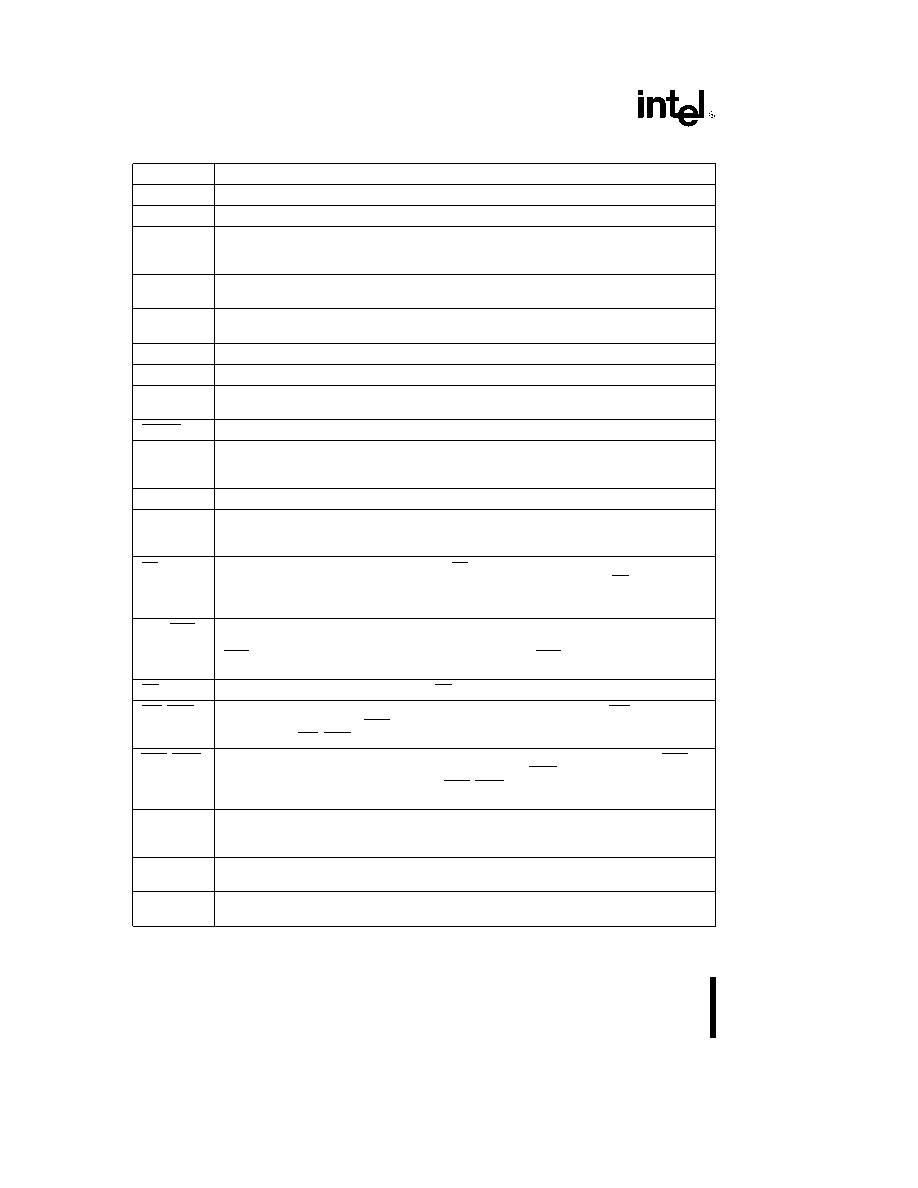
PIN DESCRIPTIONS
Symbol
Name and Function
VCC
Main supply voltage (5V).
VSS
Digital circuit ground (0V). There are multiple VSS pins, all of which must be connected.
VREF
Reference voltage for the A/D converter (5V). VREF is also the supply voltage to the analog
portion of the A/D converter and the logic used to read Port 0. Must be connected for A/D
and Port 0 to function.
ANGND
Reference ground for the A/D converter. Must be held at nominally the same potential as
VSS.
VPP
Timing pin for the return from powerdown circuit. This pin also supplies the programming
voltage on the EPROM device.
XTAL1
Input of the oscillator inverter and of the internal clock generator.
XTAL2
Output of the oscillator inverter.
CLKOUT
Output of the internal clock generator. The frequency of CLKOUT is
the oscillator
frequency.
RESET
Reset input and open drain output.
BUSWIDTH
Input for buswidth selection. If CCR bit 1 is a one, this pin selects the bus width for the bus
cycle in progress. If BUSWIDTH is a 1, a 16-bit bus cycle occurs. If BUSWIDTH isa0an
8-bit cycle occurs. If CCR bit 1 is a 0, the bus is always an 8-bit bus.
NMI
A positive transition causes a vector through 203EH.
INST
Output high during an external memory read indicates the read is an instruction fetch. INST
is valid throughout the bus cycle. INST is activated only during external memory accesses
and output low for a data fetch.
EA
Input for memory select (External Access). EA equal high causes memory accesses to
locations 2000H through 9FFFH to be directed to on-chip ROM/E PROM. EA equal low
causes accesses to those locations to be directed to off-chip memory. Also used to enter
programming mode.
ALE/ADV
Address Latch Enable or Address Valid output, as selected by CCR. Both pin options
provide a signal to demultiplex the address from the address/data bus. When the pin is
ADV, it goes inactive high at the end of the bus cycle. ALE/ADV is activated only during
external memory accesses.
RD
Read signal output to external memory. RD is activated only during external memory reads.
WR/WRL
Write and Write Low output to external memory, as selected by the CCR. WR will go low for
every external write, while WRL will go low only for external writes where an even byte is
being written. WR/WRL is activated only during external memory writes.
BHE/WRH
Bus High Enable or Write High output to external memory, as selected by the CCR. BHE will
go low for external writes to the high byte of the data bus. WRH will go low for external
writes where an odd byte is being written. BHE/WRH is activated only during external
memory writes.
READY
Ready input to lengthen external memory cycles, for interfacing to slow or dynamic
memory, or for bus sharing. When the external memory is not being used, READY has no
effect.
HSI
Inputs to High Speed Input Unit. Four HSI pins are available: HSI.0, HSI.1, HSI.2 and HSI.3.
Two of them (HSI.2 and HSI.3) are shared with the HSO Unit.
HSO
Outputs from High Speed Output Unit. Six HSO pins are available: HSO.0, HSO.1, HSO.2,
HSI.3, HSO.4 and HSO.5. Two of them (HSO.4 and HSO.5) are shared with the HSI Unit.
8
相關(guān)PDF資料 |
PDF描述 |
|---|---|
| SB83C196NP | 16-BIT, MROM, 25 MHz, MICROCONTROLLER, PQFP100 |
| SB83C196NU50 | 16-BIT, MROM, 50 MHz, MICROCONTROLLER, PQFP100 |
| SB87C196NP | 16-BIT, OTPROM, 25 MHz, MICROCONTROLLER, PQFP100 |
| S87C196NP | 16-BIT, OTPROM, 25 MHz, MICROCONTROLLER, PQFP100 |
| SC104013VFU | 16-BIT, FLASH, 40 MHz, MICROCONTROLLER, PQFP80 |
相關(guān)代理商/技術(shù)參數(shù) |
參數(shù)描述 |
|---|---|
| SB84 | 制造商:n/a 功能描述:Ships in 2 days |
| SB840 | 制造商:World Products 功能描述: 制造商:Lite-On Semiconductor Corporation 功能描述:SCHOTTKY BARRIER RECTIFIERS |
| SB840 _T0 _10001 | 制造商:PanJit Touch Screens 功能描述: |
| SB840_T0_10001 | 制造商:PanJit Touch Screens 功能描述: |
| SB840CT | 制造商:PACELEADER 制造商全稱:PACELEADER INDUSTRIAL 功能描述:ISOLATION SCHOTTKY BARRIER RECTIFIER |
發(fā)布緊急采購,3分鐘左右您將得到回復。