- 您現(xiàn)在的位置:買賣IC網(wǎng) > PDF目錄383804 > SAA7708H (NXP Semiconductors N.V.) Car Radio Digital Signal Processor PDF資料下載
參數(shù)資料
| 型號(hào): | SAA7708H |
| 廠商: | NXP Semiconductors N.V. |
| 元件分類: | 數(shù)字信號(hào)處理 |
| 英文描述: | Car Radio Digital Signal Processor |
| 中文描述: | 汽車無線電數(shù)字信號(hào)處理器 |
| 文件頁數(shù): | 24/60頁 |
| 文件大小: | 281K |
| 代理商: | SAA7708H |
第1頁第2頁第3頁第4頁第5頁第6頁第7頁第8頁第9頁第10頁第11頁第12頁第13頁第14頁第15頁第16頁第17頁第18頁第19頁第20頁第21頁第22頁第23頁當(dāng)前第24頁第25頁第26頁第27頁第28頁第29頁第30頁第31頁第32頁第33頁第34頁第35頁第36頁第37頁第38頁第39頁第40頁第41頁第42頁第43頁第44頁第45頁第46頁第47頁第48頁第49頁第50頁第51頁第52頁第53頁第54頁第55頁第56頁第57頁第58頁第59頁第60頁
1998 May 19
24
Philips Semiconductors
Preliminary specification
Car Radio Digital Signal Processor
SAA7708H
10.8.6
P
OWER OFF PLOP SUPPRESSION
To reduce the chance of plops in a power amplifier, the supply voltage of the analog part of the D/A converter can be fed
from the 5V via a transistor. An capacitor is connected to the 3.3 V to provide still power to the analog part the moment
the digital is switching off fast. In this case the output voltage will decrease gradually allowing the power amplifier some
extra time to switch off without audible plops.
10.8.7
T
HE
I
NTERNAL
VREFDA
PIN
With two internal resistors half the supply voltage VDDA2 is obtained and coupled to an internal buffer. This reference
voltage is used as DC voltage for the output operational amplifiers and as reference for the DAC. In order to obtain the
lowest noise and to have the best ripple rejection, a filter capacitor has to be added between this pin and ground.
10.8.8
S
UPPLY OF THE ANALOG OUTPUTS
All the analog circuitry of the DACs and the OPAMPS are fed by 2 supply pins, VDDA2 and VSSA2. The VDDA2 must
have sufficient decoupling to prevent THD degradation and to ensure a good Power Supply Rejection Ratio. The digital
part of the DAC is fully supplied from the chip core supply.
10.9
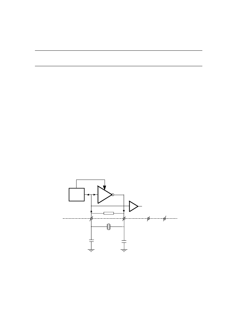
Clock circuit and oscillator
The chip has an on board crystal clock oscillator. The block schematic of this Pierce oscillator is shown in Fig. 9. The
active element needed to compensate for the loss resistance of the crystal is the block Gm. This block is placed between
the external pins OSC_IN and OSC_OUT. The gain of the oscillator is internally controlled by the AGC block. A sine-wave
with peak to peak voltage close to the oscillator power supply voltage is generated. The AGC block prevents clipping of
the sine-wave and therefore the higher harmonics are as low as possible. At the same time the voltage of the sine wave
is as high as possible which reduces the jitter going from sine wave to clock signal.
Fig. 9 Block diagram oscillator circuit
OSC_OUT
OSC_IN
VDD_OSC
VSS_OSC
Gm
AGC
ON CHIP
OFF CHIP
Rbias
Cx1
Cx2
CLOCK_TO_CIRCUIT
相關(guān)PDF資料 |
PDF描述 |
|---|---|
| SAL175UF-A | HERMETIC ULTRAFAST DIODE |
| SAL200UF-A | HERMETIC ULTRAFAST DIODE |
| SAL225UF-A | HERMETIC ULTRAFAST DIODE |
| SAL250UF-A | HERMETIC ULTRAFAST DIODE |
| SAL175UF3A | HERMETIC ULTRAFAST DIODE |
相關(guān)代理商/技術(shù)參數(shù) |
參數(shù)描述 |
|---|---|
| SAA7709/N107 | 制造商:PHILIPS-SEMI 功能描述: |
| SAA7709H/N103 | 功能描述:音頻 DSP DIGITAL SIGNAL PROCESSOR RoHS:否 制造商:Texas Instruments 工作電源電壓: 電源電流: 工作溫度范圍: 安裝風(fēng)格: 封裝 / 箱體: 封裝:Tube |
| SAA7709H/N103,518 | 功能描述:音頻 DSP DIRAC-2 RoHS:否 制造商:Texas Instruments 工作電源電壓: 電源電流: 工作溫度范圍: 安裝風(fēng)格: 封裝 / 箱體: 封裝:Tube |
| SAA7709H/N103,557 | 功能描述:音頻 DSP DIGITAL SIGNAL RoHS:否 制造商:Texas Instruments 工作電源電壓: 電源電流: 工作溫度范圍: 安裝風(fēng)格: 封裝 / 箱體: 封裝:Tube |
| SAA7709H/N103/S420 | 功能描述:音頻 DSP Car radio Digital Signal Processor RoHS:否 制造商:Texas Instruments 工作電源電壓: 電源電流: 工作溫度范圍: 安裝風(fēng)格: 封裝 / 箱體: 封裝:Tube |
發(fā)布緊急采購,3分鐘左右您將得到回復(fù)。